- News
5 March 2012
QD solar cell beats short-circuit current of reference GaAs device
Researchers from the UK and Spain have increased the performance of indium arsenide (InAs) quantum dot solar cells by varying the growth temperature [F. K. Tutu et al, J. Appl. Phys., vol111, p046101, 2012]. The participating institutions were University College London, Sharp Laboratories of Europe Ltd, Spain’s Centro Andaluz Superior de Estudios Marinos (CASEM, Andalusian Centre for Marine Studies), and the University of Oxford.
Quantum dot (QD) devices have been explored extensively as a means to improve conversion efficiencies for both emission and absorption. While 3- to 5-layer QD structures are adequate for laser diodes, photovoltaic applications need far larger active volumes of about 30 layers. In such structures, it can be particularly tricky to avoid defects.
The QD solar cells (QDSCs) were grown using solid-source molecular beam epitaxy (SS-MBE) on n-type gallium arsenide (n-GaAs) substrates. The active region consisted of 30 layers of InAs/InGaAs dots in a p-i-n structure. A dot layer was made up of 2.2 monolayers of InAs grown on 2nm of In0.15Ga0.85As and then capped with 4.5nm of In0.15Ga0.85As. The InAs layer tends to break up/self-assemble into dots.
The layers were spaced with 29nm of GaAs to give a dots-in-a-well structure (DWELL). The i-region was completed with 25nm of GaAs before deposition of the p-layers. The InAs QD density was estimated to be 5.5x10¹⁰/cm2.
The p-type and n-type emitter regions were 400nm and 3000nm, respectively. Further p-type layers consisted of a 43nm aluminum gallium arsenide (AlGaAs) window and a 1000nm p+-GaAs contact.
Three device types were produced: a reference without QDs, one where the active region was grown at constant temperature, and one where the spacer regions were grown at higher temperature than the dots. The dot growth temperature was 510°C in both the latter cases. In the high-growth-temperature spacer layer (HGTSL) device, the first 3nm was grown at 510°C and the final 26nm at 580°C.
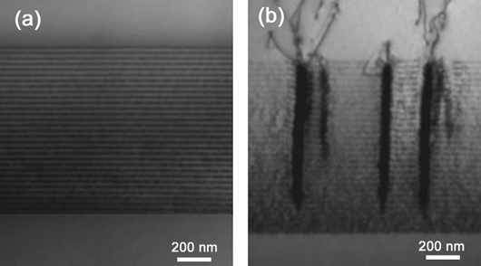
Figure 1. Dark-field (200) cross-sectional TEM images of 30-layer InAs/GaAs QDSC structures (a) with and (b) without HGTSL. The growth direction is in the vertical direction for these two images.
The effect of the HGTSL was to remove threading dislocations (TDs) from the structure (Figure 1). The non-HGSTL had severe TDs from the fifth layer, and in these layers the QD density was reduced, along with an increase in size variation. The difference is attributed to a rougher surface for low-temperature GaAs, leading to nucleation of larger InAs islands when the next layer of dots is initiated.
Photoluminescence experiments gave peak emissions for the HGTSL at wavelengths of 1100nm and 1230nm for 10K and room-temperature measurements, respectively.
Standard techniques converted the epitaxial material into solar cells with gold-zinc-gold p-contacts and indium germanium alloy-gold n-contacts.
Solar cell |
Jsc |
Voc |
FF |
η |
GaAs reference cell |
19.53 |
0.95 |
65 |
12.04 |
QDSC with HGTSL |
20.17 |
0.71 |
71 |
10.12 |
QDSC without HGTSL |
3.75 |
0.59 |
62 |
1.36 |
Table 1: Short-circuit current (Jsc), open-circuit voltage (Voc), fill factor (FF), and efficiency (η) for QDSC with and without HGTSL and GaAs SC under 1 sun air-mass (AM) 1.5 illumination.
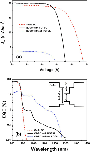 Although the HGTSL cell had improved performance over the non-HGTSL device, both had degraded overall performance compared with the GaAs reference (Table 1 and Figure 2a). The researchers comment: “This reduction of efficiency in both cases of the QDSCs with and without HGTSL is likely due to the fact that carrier lifetime in QDs is smaller than in bulk GaAs”.
However, the HGTSL cell did have the best short-circuit current of the three devices at 20.17mA/cm2. The lower open-circuit voltage is attributed to narrowing of the bandgap due to the introduction of the InGaAs quantum wells (Figure 2b inset). High short-circuit current is desirable in multi-junction devices, where currents between the devices need to be matched.
Figure 2: (a) Current density vs voltage curves of InAs/GaAs QDSCs with and without HGTSL and the reference GaAs solar cell. (b) External quantum efficiency (EQE) of InAs/GaAs QDSCs with and without the HGTSL and the reference GaAs solar cell. Inset: schematic band diagram of InAs/InGaAs dot-in-a-well structure.
External quantum efficiency (EQE) measurements show absorption in the GaAs cells only above the bandgap, creating the drop beyond 870nm (Figure 2b), while the QD structures absorb up to 1240nm. The higher current in the HGTSL device is attributed to extended absorption at wavelengths longer than the GaAs bandgap.
The higher absorption of the non-HGTSL device at the longer wavelengths is the subject of further investigations. An explanation in terms of the reduced thermal activation energy of carriers in these devices is tentatively offered.
The author Mike Cooke is a freelance technology journalist who has worked in the semiconductor and advanced technology sectors since 1997.