- News
25 May 2012
Vertical-stand surface-roughened nitride LEDs with 118.5% increased output
Researchers in China have used a combination of surface texturing and vertical-stand mounting to increase light output from nitride semiconductor LEDs by up to 118.5% [T. B. Wei et al, IEEE Electron Device Letters, published online 7 May 2012]. The researchers were based at Chinese Academy of Sciences’ Semiconductor Lighting Technology Research and Development Center, Institute of Semiconductors, and at Tsinghua University.
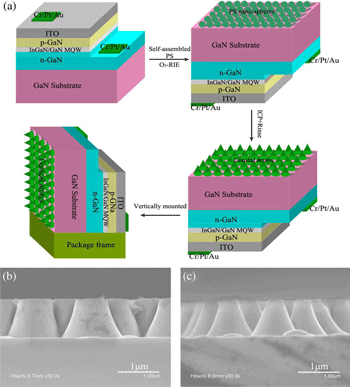 The LED epitaxial structures were grown on 350μm two-sided polished c-face free-standing GaN substrates using metal-organic chemical vapor deposition (MOCVD) – see Figure 1a. Indium tin oxide (ITO) was used as a transparent conductor on the p-GaN top surface. A diode mesa was then etched and contact electrodes applied.
The backside was textured by spin-on of polystyrene (PS) balls and inductively coupled plasma–reactive ion etch. After removal of the PS residue, the GaN surface consisted of truncated conical shapes. The purpose of such texturing is to scatter the light at different angles, allowing more light to eventually emerge from the structures. Flat GaN–air interfaces have a very narrow escape cone for light of around 23°, due to the large difference in refractive index (2.5:1).
Figure 1: (a) Fabrication flowchart of a VLED with the self-organized conical arrays on an N-face GaN substrate. Cross-sectional view of (b) truncated cone and (c) cone fabricated on LED backside by ICP etching.
The amount of truncation of the conical structures was controlled by factors such as etch time and gas flow, and the PS sphere size. The researchers investigated truncated and almost untruncated conical layers to increase light output. In both cases, the average cone base diameter was around 1.2μm and the height was 1μm.
Square LED chips measuring 1mm were mounted vertically (i.e. on their sides) in TO-cans with the n-contact up to avoid short circuits. The attachment of the GaN chip sidewall to the package frame was made with high thermal conductivity silver paste. Conventional LEDs were also planar-mounted without mirrors for comparison. The vertical mounting allowed light to escape from both sides of the chip.
While the electrical performance was similar, the light output powers of the vertical-stand devices were increased over those of the planar comparison LEDs (Figure 2). For flat backside devices the increase in light output at 20mA current injection was 16.5%. In the planar arrangement, the ‘conical’ anti-reflection layer gave 39.8% enhancement, and the truncated cone layer only 12.1%. The vertical-stand arrangement showed improved performance over the corresponding planar-mounted devices of 56.1% and 48.9%, respectively. The full enhancements over the planar-mounted device with flat back-side were 118.5% for the vertical device with conical layer and 66.8% for the truncated cones.
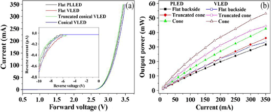
Figure 2.: Comparison of (a) forward current–voltage and (b) light output power–current characteristics of planar (PLEDs) and various fabricated vertical-stand (VLEDs) LEDs. Inset: reverse current–voltage characteristics.
The devices also benefit from the better thermal conductivity of GaN over sapphire, showing reduced thermal degradation effects up to 350mA current. Also, the red-shift of the peak wavelength is small, at 0.7nm for the planar-mounted devices and 1.9nm for the vertical-stand devices.
Angular emission studies suggest that the VLEDs emit more light through their p-GaN surfaces, compared with roughened N-faces where the conical structures are formed.
LEDs VLED GaN GaN substrate MOCVD
The author Mike Cooke is a freelance technology journalist who has worked in the semiconductor and advanced technology sectors since 1997.