

- News
1 November 2012
NGK develops GaN wafers that nearly double green LED efficiency
NGK Insulators Ltd of Nagoya, Japan has developed gallium nitride (GaN) wafers that significantly reduce defects and approximately double the luminous efficiency of green light-emitting diodes (LEDs) over previous models.
The GaN wafers have low defect density across the entire 2-inch diameter of the surface, as well as having a colorless transparency. NGK says that it achieved this through proprietary improvements to liquid phase epitaxy (LPE) technology for single-crystal growth.
In joint research with Nagoya University, green LED chips formed on NGK’s GaN wafers showed internal quantum efficiency of 60% (for an injection current density of about 200A/cm2). This is roughly double that of green LED chips currently on the market, it is reckoned. The results were jointly announced at the International Workshop on Nitride Semiconductors 2012 (IWN 2012) in Sapporo, Hokkaido, Japan (14-19 October).
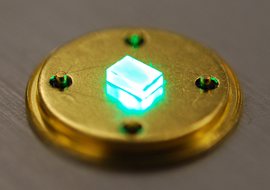 Picture: LED chip under test - facet size, 0.3mm x 0.3mm; injection current, 200mA; central wavelength, 525nm.
In previous LED chips using sapphire substrates, defects in the light-emission layer have been common, especially for green LEDs, says NGK. These defects limited operating current, which in turn prevented the LEDs from achieving sufficient brightness.
NGK says that this issue can be addressed by using its low-defect GaN wafers as substrates, enabling dramatically improved quality of the light-emission layer. The resulting reduction in current loss allows a higher current, making high-brightness green LEDs a reality. When these are used to make up green LED light sources, the result is a more than 20-fold improvement in brightness compared with previous models, says NGK. Light sources can also be made more compact due to the simplified heat dissipation structure (since less heat is generated from current loss). This control of heat-related degradation also enables longer product life, the firm adds.
The realization of high-brightness (HB) green LED light sources means that HB-LED light sources are now available for all three primary colors of light (red, green and blue). “We can thus expect to see advancements in the development of new applications for LEDs, specifically for use in projectors and other imaging applications,” says NGK.
This emerging potential for green LED applications follows NGK’s announcement in April of applications for blue LEDs. NGK says that is now poised to also apply its technology to inverters used in hybrid and electric vehicles, power amplifiers for wireless communications base-stations, and other power devices. NGK hence aims to take steps to further reduce defect density in its GaN wafers, and to produce larger wafers (greater than 6-inches in diameter).
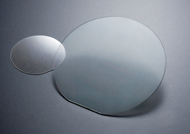 Picture: GaN wafers: (left) 2-inch diameter and (right) 4-inch diameter.
Sample shipments of 2-inch-diameter wafers are already underway, with 4-inch wafers set to follow before the end of 2012. Monthly production capacity is planned to increase from the current level of 200 wafers (2-inch wafer) to more than 1000 wafers during fiscal 2012. By 2014, NGK aims to have a wide-ranging line-up of wafers, extending from 2- to 6-inch diameter, ready for LED and power device applications.
NGK’s GaN substrate yields HB-LED chip with 90% IQE at 200mA
NGK introduces LPE-grown GaN substrate for UHB-LED applications