

- News
1 November 2012
One-step gallium nitride on sapphire through graphene coating
Researchers in Korea have been studying how to simplify gallium nitride (GaN) growth on sapphire through use of an initial graphene layer [Jae-Kyung Choi et al, Nanotechnology, vol23, p435603, 2012]. The researchers were based at Ulsan National Institute of Science and Technology (UNIST), Seoul National University, and Sogang University.
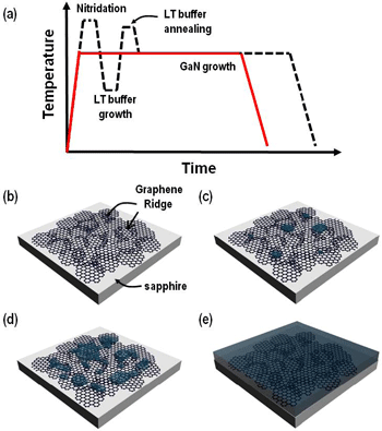 The graphene layer improves wetting between the GaN and sapphire, allowing a one-step high-temperature process to be used instead of the more complicated sequences of low- and high-temperature growth normally implemented to initiate crystalline GaN growth (Figure 1a).
Figure 1: (a) Sketch of conventional two-step process (black dotted line) compared with one-step process using ultrathin graphene coating layers (red line), (b)–(e) scheme of one-step growth of epitaxial GaN films using ultrathin graphene coating layers: (b) graphene coating on sapphire substrate by DAS process; (c) GaN nucleation along naturally formed multilayer graphene ridges; (d) lateral growth of GaN on a graphene coating layer; (e) full coalescence of GaN on a graphene/sapphire template.
Although by some measures the quality of the GaN film is not as good as a layer grown by traditional methods, the internal quantum efficiency (IQE) of multi-quantum wells (MQWs) grown on the GaN film when subjected to photoluminescence (PL) is as high as for similar structures on conventional GaN. The researchers also believe that the method could be expanded to grow many other heteroepitaxial films on arbitrary substrates with large lattice and thermal misfits.
The researchers used their own low-temperature diffusion-assisted synthesis (DAS) process to create graphene on c-plane sapphire. DAS begins with room-temperature evaporation of polycrystalline nickel onto the sapphire. The carbon source is graphite powder that covers the substrate. The carbon-nickel/sapphire ‘diffusion couple’ is clamped at 1MPa pressure in a molybdenum holding stage. The assembly is put in a quartz tube with flowing argon gas and heated to temperatures between 160°C and 360°C for between 30 and 150 minutes. After the heat treatment the samples are cleaned and then etched with iron chloride solution to remove the nickel. The result is nanocrystalline graphene on sapphire.
A commercial low-pressure reactor was used to perform metal-organic chemical vapor deposition (MOCVD) of the GaN layer at 1040°C. The low pressure of 10-3Torr was used to repel residual oxygen from the substrate and graphene layer. The substrate was then ramped to the GaN growth temperature in a nitrogen atmosphere. Once at the growth temperature, the substrate was annealed in the same atmosphere for 5 minutes.
The source gases for the GaN MOCVD were tri-methyl-gallium (TMG) and ammonia (NH3) in hydrogen carrier. The growth pressure was 25Torr.
The researchers see the irregularity of the graphene film that results from their process as being important for GaN nucleation (Figure 1). The DAS process results in ridges of multi-layer graphene with the spacing determined by the growth conditions.
“It is known that epitaxial GaN films could not be grown on pristine graphene layers due to their chemical stability,” the researchers write. Other groups attempting to grow GaN and zinc oxide semiconductor films on graphene have introduced special protrusions, such as titanium droplets, to nucleate growth.
The researchers see their technique as having the advantage of not needing such extra processing: “We find that GaN nucleation can readily occur along the naturally formed graphene ridges, not on the basal plane of graphene, presumably because the side walls at graphene ridges contain many step-edges, which can act as nucleation sites. The next stage of GaN growth involves the lateral overgrowth on pristine graphene, taking advantage of high adatom mobility on a functional coating layer.”
 The hexagonal structure of graphene has a lattice misfit with GaN of 10.8%. The researchers see the graphene as improving the ‘wetting’ between the sapphire and GaN. The nanocrystalline graphene encourages overgrowth of GaN in a continuous, flat layer, rather than the more usual islands in the early phase of growth on sapphire.
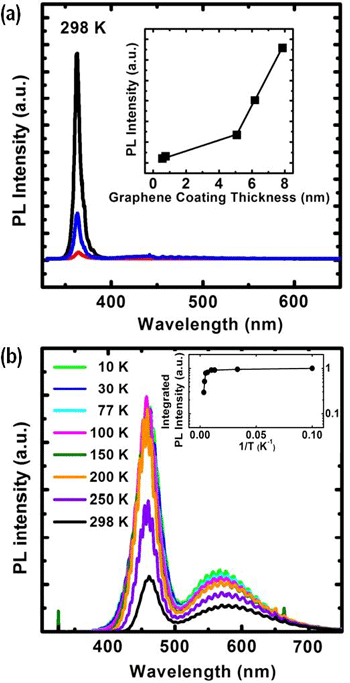
Figure 2: (a) Room-temperature PL spectra of GaN films grown on a sapphire substrate with 0.6nm-thick (red), 5.1nm-thick (blue), and 7.9nm-thick (black) graphene coating layers, respectively (from bottom to top). Inset shows changes in the integrated PL emission intensity of GaN films on graphene/sapphire template as function of graphene coating thickness. (b) Temperature-dependent PL spectra of InGaN/GaN MQWs grown on GaN/graphene/sapphire heterosystem with graphene coating thickness of 7.9nm at temperatures from 10 to 300K. Inset: Arrhenius plot of PL at 2.7eV, showing high IQE of ~0.3.
The researchers found that increasing the graphene layer thickness enabled them to achieve a nearly surface-pit-free, mirror-like GaN layer. The dislocation density of 1.2x10⁹/cm2 was less than an order of magnitude higher than that for conventional GaN layers grown on a low-temperate (Al, Ga)N buffer/sapphire template (3x10⁸/cm2). Since the crystal quality is very sensitive to MOCVD conditions, it is hoped that improvements could come from process optimization.
The researchers analyzed the GaN film using x-ray diffraction and electron micrography. Also, they carried out photoluminescence experiments using a mercury-cadmium laser excitation (Figure 2). With a view to optoelectronics (LED and LDs), the researchers also created 3-period multi-quantum wells (MQWs) of indium gallium nitride in GaN barriers on the GaN/graphene/sapphire structures. By varying the measurement temperature, the researchers determined an internal quantum efficiency value of around 0.3 (30%). The same MQW structure grown on conventional two-step growth templates gave similar performance of ~0.3 IQE.
GaN Sapphire Graphene coating MOCVD
The author Mike Cooke is a freelance technology journalist who has worked in the semiconductor and advanced technology sectors since 1997.