

- News
17 October 2012
Growing high-mobility transistors directly on silicon
Hong Kong University of Science and Technology (HKUST) has grown high-performance indium gallium arsenide (InGaAs) metal–oxide–semiconductor high-electron-mobility transistors (MOSHEMTs) directly on silicon [Xiuju Zhou et al, Appl. Phys. Express vol5, p104201, 2012]. In particular, the maximum drain current density was more than 2A/mm at a drain bias of 0.6V. The International Technology Roadmap for Semiconductors (ITRS) made such a 2A/mm specification to meet future needs for high-performance logic.
In recent years, there has been much development of III-V high-mobility-channel transistors based on InGaAs and other compound semiconductors for use as high-speed logic in mainstream electronics systems. To be a viable future technology, such devices must be incorporated in large-scale production – and that means production on large-diameter silicon wafers.
Although much progress has been made, there is still much to be done. The best performing devices tend to be grown on indium phosphide and are grown using molecular beam epitaxy (MBE). There are techniques to transfer such devices to silicon such as wafer bonding, but a preferable approach would be to grow these devices directly on silicon. Further, manufacturers would prefer more cost-effective growth techniques such as metal-organic chemical vapor deposition (MOCVD).
The HKUST device fabrication began with epitaxial growth on 4-inch exact-oriented (001) silicon using MOCVD in an Aixtron 200/4 system (Figure 1). The (001) silicon crystal orientation is that preferred in present day CMOS production.
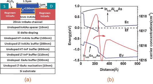
Figure 1: Schematic cross section of finished device (LT: low temperature, HT: high temperature; figure is not drawn to scale). (b) Simulation of the band structure and carrier distribution of the InAlAs/InGaAs heterostructure.
The HKUST epitaxial structure was designed to have an inverted-type InGaAs channel sandwiched between InAlAs cap and spacer layers with the peak of the electron carrier distribution nearer the channel/spacer interface. Hall measurements of the material gave a mobility of 4100cm2/V-s, carrier density of 4.02x10¹²/cm2, and sheet resistance of 379Ω/square.
 The source/drain regions were re-grown using a self-aligned process. Such re-growth is expected to improve the access resistance of the connection between the source/drain metal terminals and the channel of the transistor.
Silicon dioxide was used as passivation and re-growth mask. The mask was patterned with a buffered oxide etch and then the source/drain recess down to the InGaAs channel layer was formed using phosphoric acid/hydrogen peroxide solution in water. The recessing removed all the top InAlAs layer and 10nm of the InGaAs channel in the source/drain regions. The re-growth of silicon-doped n-InGaAs was by MOCVD.
The transistor fabrication began with buffered oxide etch to remove the silicon dioxide mask and wet etch down to the InAlAs layer for mesa isolation. The gate region was subjected to a pre-treatment with tri-methyl-aluminium (TMA) in an Oxford Instruments OpAL atomic layer deposition (ALD) tool. The pre-treatment was designed to provide passivation for improving the gate dielectric/III-V semiconductor interface. The gate dielectric of aluminium oxide was deposited using ALD, followed by annealing at 380°C.
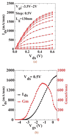
Figure 2: (a) Output characteristic of device with 130nm channel. (b) Transfer characteristics of device with 130nm channel at 0.5V drain.
The ohmic source/drain contacts consisted of nickel/germanium/gold/nickel/germanium/gold/. The gate metal stack was titanium/platinum/gold. The channel length of the resulting device was 130nm. The gate width was 9.57μm.
The maximum drain current was 2.03A/mm with a gate potential of 2V and a drain bias of 0.6V (Figure 2). Under the same bias conditions, the gate leakage was more than six orders of magnitude smaller, at 6.17x10⁻⁷A/mm. A peak extrinsic transconductance of 744mS/mm was achieved at 0.5V drain. The threshold voltage was negative at –2.9V, indicating undesired ‘normally-on’ or ‘depletion mode’ behavior. The on-resistance of 163Ω-μm is considered ‘ultra-low’ and is attributed to the “raised S/D with high doping level”.
These results are comparable with the best results for devices grown on InP (Table 1). The researchers comment: “Although the devices reported in this work were metamorphically grown on Si substrates, which inevitably have more dislocations in the active layers and rougher surface than lattice-matched ones on InP substrates, they still exhibit attractive current drivability and low Ron.”
The researchers attribute their results to their achievement of high-quality metamorphic growth of InP on silicon substrates and to the selective re-growth of the source/drain regions.
Ref. |
Gate/channel (nm) |
Substrate |
Mode |
Oxide |
Ids (mA/mm) |
Ron (Ω-μm) |
14 |
160 |
InP |
E |
Al2O3 |
467 |
1071 |
15 |
1000 |
InP |
E |
Y2O3/Al2O3 |
555 |
938 |
16 |
200 |
InP |
E |
Al2O3 |
437 |
737 |
17 |
100 |
InP |
D |
Al2O3 |
944 |
496 |
18 |
50 |
InP |
D |
Al2O3 |
2400 |
160 |
19 |
55 |
InP |
E |
Al2O3/HfO2 |
1756 |
199 |
20 |
60 |
InP |
D |
Al2O3 |
978 |
341 |
HKUST work |
130 |
Si |
D |
Al2O3 |
1920 |
163 |
Table 1: Comparison of on-resistance (Ron) and on-current (Ids) at a drain bias of 0.5V for InGaAs channel FETs (D: depletion, E: enhancement, R: reference).
The subthreshold performance was not as low as desired for applications. The subthreshold slope of 263mV/dec at 50mV drain is more than twice that obtained by other groups developing InGaAs channel devices and far off from the theoretical ideal of ~60mV/dec. “The current SS and large gate bias swing are believed to be limited by the capacitance equivalent thickness (CET) arising from the thick Al2O3 gate dielectric and InGaAs channel,” the researchers write. “More efforts are required to improve gate electrostatic control over the channel.”
The effective mobility of a 1.2μm channel device was also evaluated, showing a peak at
2975cm2/V-s.
http://apex.jsap.jp/link?APEX/5/104201
The author Mike Cooke is a freelance technology journalist who has worked in the semiconductor and advanced technology sectors since 1997.