

- News
18 October 2012
Lithium aluminate substrate for low-cost nonpolar gallium nitride
Researchers based in Germany and the Netherlands have been studying the potential for growing nonpolar gallium nitride (GaN) on lithium aluminate (LiAlO2) [Kwang-Ru Wang et al, Appl. Phys. Express, vol5, p105501, 2012].
In particular, the initial nitridation process that is used before the growth of GaN was analyzed using x-ray reflectivity (XRR) and cross-sectional high-resolution transmission electron microscopy (HRTEM). It was found that the nitridation produced a single-crystal aluminium nitride (AlN) layer without any detectable misfit dislocations. Such a layer forms a good base for further growth of nonpolar m-plane GaN.
The researchers were variously associated with Paul-Drude-Institut für Festkörperelektronik, RWTH Aachen, PANalytical B.V., and Aixtron SE.
Nonpolar GaN is of much interest for the production of high-efficiency light-emitting diodes. In normal polar c-plane GaN, large electric fields result from the large polarization fields in the c-direction. These fields interfere with the recombination process that produces light, reducing efficiency.
Unfortunately, high-quality m-plane GaN is difficult to produce because of large lattice mismatches with the well established substrates, leading to defects and dislocations. The substrates with the smallest lattice mismatch, such as silicon carbide (SiC) or free-standing GaN (FS-GaN), are usually very expensive.
Michael Heuken of RWTH Aachen and Aixtron comments: “2-inch LiAlO2 substrates can be very low cost, as less energy is needed to make them compared even with sapphire (Al2O3).” Further cost savings arise because LiAlO2 (LAO) is softer than Al2O3, reducing the consumption of cutting/lapping materials, and of time and money during manufacturing of the substrate.
Another advantage of LiAlO2 is that lift-off – i.e. separation of the GaN film from the substrate – can be practically automatic, without any further processing. The researchers find that thick nitride semiconductor layers often peel off or separate when the wafer is vacuumed off the wafer holder in the metal-organic chemical vapor deposition (MOCVD) chamber. This automatic lift-off is very attractive for lower-cost FS-GaN substrates from films grown on LiAlO2, avoiding laser or etch processes that are expensive and time consuming.
Gamma-phase (γ-phase) 2-inch wafers of LiAlO2 substrate have been commercially available for almost ten years at prices less than 10% of 2-inch m-plane SiC or less than 30% of 5mm x 10mm pieces of free-standing m-plane GaN.
Further, according to Heuken, “the supply of 6-inch SiC wafers could become limited due to strategic (military) purposes for which it has been developed in the USA. Presently, 2-inch m-plane free-standing GaN wafers are not available in the market.” Kwang-Ru Wang of Paul-Drude-Institut adds that “this may change, since technology moves very fast in this field. Also 2-inch m-plane SiC wafers, although theoretically available, are difficult to buy.”
Heuken adds: “The quality of nonpolar m-plane GaN grown on LiAlO2 is not presently as good as m-plane GaN on FS-GaN.” Wang adds: “However, our TEM data show that part of the reason for this is attributable to the quality of the LiAlO2 substrate.”
The researchers found that most of the planar defects (i.e. stacking faults) found in nonpolar GaN grown on LAO is related to surface morphology and is not related to lattice mismatch or strain relief.
Christof Mauder based at RTWH Aachen comments: “The most important origin of defects in nonpolar nitride layers is the lattice mismatch between substrate and the epitaxial layers, leading to the formation of planar stacking faults, which are detrimental to device performance. Therefore, low mismatch is a prerequisite for the growth of high-quality nonpolar m-plane GaN thin films.” However, the lattice mismatch for LiAlO2 is less than 1.7% and hence much lower than the leading alternatives such as sapphire or SiC.”
Wang adds: “Our research is important because of the challenge of quality improvement, and reproducibility is directly related to the surface sensitivity of LiAlO2 substrate during the process, as we’ve identified.”
Dr Achim Trampert, the leader of the project at Paul-Drude-Institute, comments: “The diameter of the LiAlO2 substrates, as well as the quality, needs to be improved significantly.”
Once this happens and processes are developed for reproducibly growing high-quality m-plane GaN on the resulting substrates, market demand should increase. In addition, since neither 2-inch m-plane SiC nor 2-inch m-plane GaN substrates are really available in the market right now, the research may open another achievable and low-cost way in making real 2-inch, or even larger, free-standing, nonpolar GaN substrates. With improved quality of the substrates, it is hoped that full structure, high-performance, nonpolar GaN light-emitters will be realized soon on LiAlO2.
One headache for scientists and engineers is that LiAlO2 decomposes at elevated temperature and in hydrogen environments. High-quality GaN needs to be grown at higher temperature than other III-V materials such as GaAs.
Wang comments: “Before our detailed studies, people could only follow their own empirical rules about whether to perform or not substrate pre-treatments [M.D. Reed et al, J. Cryst. Growth, vol274, p14, 2005; Chengxiang Liu et al, J. Cryst. Growth, vol298, p228, 2007]. It was anybody’s guess whether pre-treatment would be good or bad for subsequent GaN growth as it dominates the crystal orientation (c- or m-plane) and phase purity of thin films.”
“Our detailed investigations clearly demonstrate that precise control of the nitridation pre-treatment process plays a key role in creating a pure phase, high-quality m-plane GaN thin film reproducibly on this novel alternative oxide substrate with high potential for future high-performance optoelectronics applications. Our study should also guide people who cannot precisely control their initial processes, allowing them to check if their nitridated layer is a pure phase m-plane AlN layer. We see the creation of such an initial layer as being key to successful growth of high-quality m-plane nitride semiconductors on this substrate.”
 The researchers began their growth process by cleaning their γ-LiAlO2 before loading it into the metal-organic chemical vapor phase epitaxy (MOVPE) reactor. Two substrates were processed – one was subjected to a flow of ammonia at 300mbar pressure and 900°C temperature for two minutes and the other for 5 minutes. After nitridation, a layer of 1.2μm m-plane GaN was grown in a three-step process.
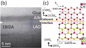
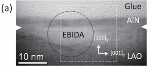
Figure 1: (a) HRTEM image of the heterointerfaces along γ-LAO[010] zone axis for sample with 5-minute nitridation process. (b) HRTEM image of central area indicated by rectangle in (a) with the vertical dashed lines representing the coherent AlN/γ-LAO heterointerface. (c) Ball-and-stick model of the AlN/γ-LAO heterointerface projected along the γ-AlN[0001] and γ-LAO[010] zone axes.
XRR and HRTEM (Figure 1) analysis determined that the longer nitridation process resulted in a single ~2nm layer of m-plane AlN. This sample also was free of misfit dislocations in a region investigated using HRTEM. By contrast, nitridation of sapphire leads to layers of AlN with dislocations due to plastic relaxation of strain as a result of the much larger mismatch of lattice parameters.
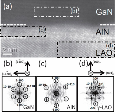
Figure 2: (a) HRTEM image of GaN/AlN/γ-LAO double heterointerface prepared with 2-minute nitridation process. (b-d) Fast Fourier transform (FFT) patterns for GaN, AlN, and γ-LAO, respectively. Crystal orientation of the NH3-induced AlN layer is exactly the same as that of the following m-GaN, which indicates that nitridation-induced, monocrystalline layer is epitaxial m-AlN. Crystal orientations of GaN and γ-LAO are indicated in (b) and (d), respectively.
In terms of the interface with the overlying GaN, the quality on top of the 2-minute nitrided film seems better, according to x-ray rocking curves and atomic force microscopy (AFM). The (1-100) x-ray rocking curves of the m-GaN films were as low as 361 arcsecs and 2566 arcsecs, respectively, parallel and perpendicular to the [0001] direction.
The researchers comment: “The achieved x-ray values are similar to values observed in much thicker m-GaN samples, which are grown by hydride vapor phase epitaxy [HVPE] using lateral epitaxy overgrowth on γ-LAO and m-plane 6H-SiC substrates [B. A. Haskell et al, Appl. Phys. Lett. vol86, p111917, 2005].”
http://apex.jsap.jp/link?APEX/5/105501
The author Mike Cooke is a freelance technology journalist who has worked in the semiconductor and advanced technology sectors since 1997.