- News
4 September 2012
Wafer-scale transfer of III-Vs to silicon preparing for low-cost manufacturing
Researchers based in the Republic of Ireland, Northern Ireland and the USA have developed a wafer-scale method to integrate III-V devices with silicon and other substrates [John Justice et al, Nature Photonics, published online 19 August 2012]. The researchers were based at Ireland’s Tyndall National Institute, University College Cork, Ireland, Semprius Inc of North Carolina, and Seagate Technology, Northern Ireland.
The team foresees applications arising within the hard-drive and more general electronics industries. For hard-drives, the new heat-assisted magnetic recording (HAMR) technology uses a laser light sources to increase storage densities. Seagate reported the achievement of 1terabit/inch2 density in March this year. This application requires III-V laser diodes integrated with alumina/titanium carbide (AlTiC) substrates. Another potential application is increased signal data rates for CMOS-based circuits on silicon.
The researchers comment: “These and other forthcoming applications will require laser device volumes that are multiples of those in use today. A prerequisite for any design is that the laser can be efficiently integrated with the low-cost manufacturing infrastructure and planar processes already established for AlTiC and silicon substrates.”
The new wafer-scale method involved transferring epitaxial material ‘coupons’ from a III-V wafer to the new substrate in batches. The transferred material is then processed into III-V laser diodes.
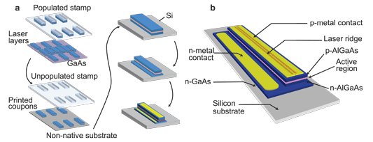
The epitaxial material was supplied by IQE Ltd. The structure grown by metal-organic chemical vapor deposition (MOCVD) consisted of two compressively strained aluminium indium gallium arsenide (AlInGaAs) wells in aluminium gallium arsenide (AlGaAs). The AlGaAs sacrificial buffer layer before the laser structure was 1μm thick with 95% Al-content.
Coupons were formed with photolithography and wet etch. The coupons were separated from the underlying sacrificial layer with hydrochloric acid before transfer printing. The coupons were kept in place on the substrate using photoresist resin.
The transfer printing was performed using a microfabricated stamp consisting of elastomer and glass layers. The stamp mounted on a precision motion platform was designed to pick up coupons from alternate rows and columns. Four passes of the stamp removes all coupons from the original substrate. The stamp contained 16x23 coupons per print. The pitches of the 400μm x 100μm coupons were 420μm x 175μm on the III-V wafer and 840μm x 350μm on the stamp.
The printing step consisted of a shear-enhanced transfer process creating Van der Waals bonds between coupon and new substrate. The process has been performed on silicon and alumina/titanium carbide (AlTiC). A 1μm polymer layer of Dow Cyclotene (BCB) was coated onto the wafer before transfer printing to enhance transfer-printing yields.
The laser formation consisted of facet and waveguide formation. The facets were etched with a silicon tetrachloride/helium inductively couple plasma using a silicon dioxide mask. Waveguide ridges with widths of 3μm and 6μmm were etched to a depth of 1.6μm, 50nm above the top of the core waveguide layers. The ridges did not extend to the edges to avoid facet damage. The p-contact consisted of titanium/platinum gold.
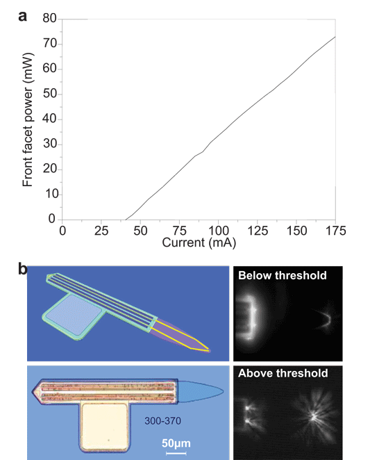
There was some degradation in laser performance from the process: the laser threshold was higher, at 17mA, compared with 14mA for a cleaved-facet device on GaAs substrate. Total slope efficiency was 0.62W/A on silicon and 0.8W/A on GaAs. The wavelength of the devices was 824nm (near-infrared). The small-signal modulation bandwidth was more than 3GHz.
The researchers comment: “The difference in characteristics can be explained by the experimental collection efficiency not being as high for the device on silicon, as well as by the different levels of current injection on the etched facet devices where the ridge waveguide and the p-type contact are recessed from the facet.”
The researchers had been hoping for improved thermal performance due to the higher thermal conductivity of silicon compared with GaAs. However, the thermal resistivity of the device on silicon fell in the range 20-40K/W typical of GaAs-based devices. The team believes the disappointing result is due to the heat-generating region of the III-V device being too far from the silicon material. The present distance was 4μm, whereas simulations suggest that this needs to be reduced to less than 3μm for the silicon to be effective in conducting heat away from the device.
The collaborators also produced external cavity laser diodes with output power of 60mW External waveguides were formed using a silicon dioxide lower cladding applied with plasma-enhanced chemical vapor deposition (PECVD). The upper part of the waveguide consisted of spin-on PMGI SF11 photoresist, patterned with ultraviolet lithography.
III-V laser diodes IQE MOCVD AlInGaAs wells AlGaAs
The author Mike Cooke is a freelance technology journalist who has worked in the semiconductor and advanced technology sectors since 1997.