

- News
11 April 2013
Fraunhofer-IAF’s GaN X-band amplifier to be launched aboard ESA’s Proba-V earth observation mini-satellite
The launch by the European Space Agency (ESA) of its Proba-V earth observation mini-satellite in the coming weeks will represent the first time that a European-made device based on gallium nitride (GaN) will be sent into space. This follows an intensive test series that has qualified the amplifier - developed by the Fraunhofer Institute for Applied Solid State Physics IAF in Freiburg, Germany - for launch into space.
 Picture:
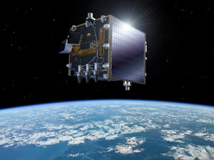
The Proba-V mini-satellite will send pictures of the earth’s vegetation from space. © ESA – P. Carril
Picture:
The Proba-V mini-satellite will send pictures of the earth’s vegetation from space. © ESA – P. Carril
The satellite weighs about 140kg and is just about the size of a washing machine. The mini-satellite Proba-V is covered in solar cells and will be observing the vegetation on earth. Every other day, the environmental satellite will send pictures from a distance of about 820km. Rain forest destruction, pollution of the seas and soil erosion will be made visible by pictures taken in various spectral ranges.
Being more robust, more compact and lighter than traditional solutions, the new GaN technology promises to significantly improve communication electronics in space. “We expect signal strength and data transmission to improve five- or tenfold,” says Andrew Barnes, who is responsible for the project at ESA. Based on GaN high-electron-mobility transistors (HEMTs), the amplifier circuit operates in the 8–8.5GHz (X-band) frequency range for Proba-V’s communication system. Tesat-Spacecom GmbH of Backnang, Germany, in cooperation with SCHOTT Electronic Packaging, packaged the amplifier together with further components into a hermetically sealed housing suitable for operation in space. “We are eagerly awaiting the results of the first practical test in space,” says Barnes.
 Picture:
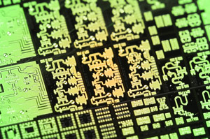
Processed GaN-based X-band amplifier circuit for Proba-V, measuring just 2mm x 3.5mm. © Fraunhofer IAF
Picture:
Processed GaN-based X-band amplifier circuit for Proba-V, measuring just 2mm x 3.5mm. © Fraunhofer IAF
GaN robust and reliable in stress tests
GaN devices can be operated under much higher voltages and temperatures than traditional silicon or gallium arsenide (GaAs) components. The circuits are more compact, smaller and lighter than other solutions, and may even replace electron tubes currently used for amplification. This would significantly reduce weight and transport costs, which can amount to €30,000/kg of payload. Due to the long lifetime and radiation hardness of the material, such electronic devices are suited to the extreme conditions posed by aerospace.
However, before being authorized for space travel, the GaN device had to prove its resilience. It was exposed to cold and heat, strong vibration and motion as well as radiation. “Accelerated lifetime tests, conducted together with Tesat-Spacecom, have shown that our gallium nitride amplifier will live for at least 20 years,” says Dr Patrick Waltereit, project leader at Fraunhofer IAF. “The approval of our device for the flight into space is an important milestone for the further development of gallium nitride technology, also for other areas of application,” he adds.
Pushing the limits of silicon technology
Due to its exceptional physical properties, GaN is suited to applications in power electronics, says Fraunhofer IAF. Compared with semiconductors such as silicon and GaAs, GaN has a larger bandgap (3.4eV) and higher breakdown field strength (3.3MV/cm). Higher dielectric strength and current density result in a fivefold increase in power density. Moreover, the usable frequency range is larger in GaN, allowing several functions to be integrated on one chip. Also, GaN’s thermal robustness results in a considerable decrease in cooling effort, which is both energy- and cost-efficient. This makes compact and energy-efficient GaN devices interesting not only for applications in aeronautics but also for voltage converters for the batteries of electric cars, solar panels or household appliances. Fraunhofer IAF says that the devices hence offer great potential especially for applications that demand high performance and long lifetime even in harsh environmental conditions (where silicon technology meets its limits).
The project is part of the initiative Great² (‘GaN Reliability Enhancement and Technology Transfer Initiative’), which ESA established to exploit the potential of GaN technology for aeronautics. Together with industrial partners, research institutes involved in III-V semiconductors such as Fraunhofer IAF develop high-quality GaN-based devices under the project leadership of Tesat-Spacecom, witn the aim of strengthening the competitiveness of the European aerospace industry.
