


- News
9 August 2013
Increased maximum oscillation for ETH double-heterostructure transistor
ETH-Zurich has reported increased maximum oscillation frequency for its indium phosphide/gallium arsenide antimonide (InP/GaAsSb) double-heterostructure bipolar transistors (DHBTs) [Rickard Lövblom et al, IEEE Electron Device Letters, published online 12 July 2013].
Based on radio-frequency measurements between 0.2GHz and 40.2GHz, the researchers extrapolated a cut-off frequency (fT) of 428GHz and a maximum oscillation (fMAX) of 621GHz. “To the best of our knowledge, this represents the highest fMAX reported for any InP/GaAsSb DHBT,” the researchers write. The performance beats ETH’s previous device by 100GHz for fMAX [reported ETH solves InP/GaAsSb maximum oscillation bipolar disorder].
The epitaxial material (Figure 1) was grown on 2-inch semi-insulating indium phosphide (InP) substrate using metal-organic chemical vapor phase epitaxy. The InP and GaAsSb have a staggered ‘type-II’ band alignment where the conduction and valence band offsets are in the same direction at interfaces. The material design had a zero conduction band offset at the base-emitter junction and 150meV offset at the base-collector junction.
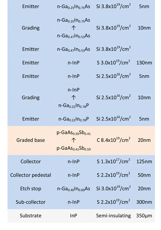
Figure 1: Epitaxial layer structure.
The devices were built using a triple mesa process. The emitter contact was 0.3μm wide and the base was 0.5μm. The emitter-base junction width was 0.2μm, giving an emitter area of 0.2μm x 4.4μm. The structure was achieved using electron-beam lithography and a hybrid dry/wet etch.
The emitter electrode metals were titanium/platinum/gold. The base electrode consisted of platinum/nickel/platinum/gold.
The emitter sidewall and base extrinsic surface were passivated with silicon nitride. Undercut etching was used to reduce the length of the collector mesa with the aim of decreasing the extrinsic base-collector capacitance.
Application of the final metal interconnects was preceded by a low-temperature (less than 190°C) Teflon-based etch-back planarization developed at ETH [Teflon and III-V double heterostructure transistors].
The high fMAX performance was attributed to the small emitter width of 0.2μm and the reduced extrinsic base-collector capacitance. Improvement in fT over other devices produced by ETH was attributed to “a higher Kirk current density achieved by raising the collector doping level.”
The Kirk effect in bipolar transistors is a significant increase at high current densities of the transit time across the base region, degrading device performance. A higher Kirk current density means a delay in the onset of the effect.
The bias conditions for the quoted frequency cut-offs were 7.6mA collector current and 1.2V between collector and emitter. Varying these conditions (Figure 2) decreased the cut-off frequency but increased fMAX to 634GHz (1.6V collector-emitter).
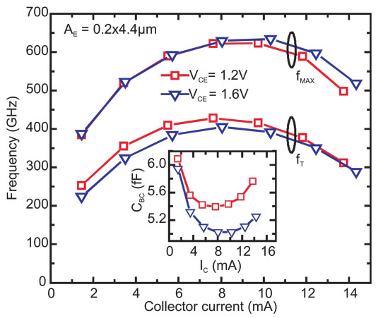
Figure 2: Dependence of fT and fMAX on collector current at 1.2V and 1.6V collector-emitter biases. Inset: total base-collector capacitance as a function of collector current.
The DC peak current gain of the device was 19 and the common-emitter breakdown voltage (BVCEO) was 5V at 1kA/cm2 collector current density.
InP GaAsSb DHBT DHBT InP substrate GaAsSb
http://ieeexplore.ieee.org/xpl/articleDetails.jsp?arnumber=6558475
The author Mike Cooke is a freelance technology journalist who has worked in the semiconductor and advanced technology sectors since 1997.
