


- News
30 August 2013
Tunneling to avoid efficiency droop in nitride semiconductor LEDs
Ohio State University is proposing the use of a newly developed tunnel junction as a means to ameliorate the effects of efficiency droop in nitride semiconductor light-emitting diodes (LEDs) and other optoelectronic devices [Fatih Akyol et al, Appl. Phys. Lett., vol103, p081107, 2013].
The peak efficiency point of such devices can be as low as a few milliamps, with the power rating in the tens of milli-watt range. For general illumination one needs devices operating at the order of 1 Watt of power. The result is that LED bulbs need a large number of LEDs – around 100 if operating at peak efficiency. Economic constraints lead to trade-offs between production costs and efficiency.
The Ohio proposal would be to cascade a series of LEDs in a vertically integrated monolithic structure with a number of devices coupled in series and operated at low current injection while a high voltage is applied across the whole assembly.
In such a structure, one needs to overcome the fact that the top p-type contact of one device would be under the n-type region of the next. Simply depositing the n-type contact on the p-type contact would set up a reverse-biased diode that would resist current flow.
The new tunnel junction [Sriram Krishnamoorthy, Nano Lett., vol13, p2570, 2013] is proposed as an ohmic link between the devices. The junction would feed/regenerate holes into the p-type region and electrons into the n-type region. For such a tunnel junction to work effectively it has to offer as small as possible resistance to current flow in the desired direction.
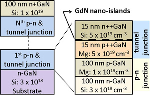 Figure 1: Epitaxial design of the cascaded p-n junctions.
The Ohio group produced a proof-of-concept where the tunnel junction is used to link a series of p-n diodes rather than LEDs (Figure 1). The structure was constructed using plasma-enhanced molecular beam epitaxy (MBE) on free-standing n-type gallium nitride (GaN) substrates. The tunnel junctions were combined with p-n junctions with up to four repeats. The tunnel junctions consisted of gadolinium nitride (GdN) nano-islands sandwiched between heavily doped p- and n-type gallium nitride.
The material stack was formed into mesa-type diodes with an area of 100μm2. The top and bottom n-GaN regions were contacted with ohmic aluminium/gold metal.
The diode cascades demonstrated rectifying behavior. The turn-on voltage increased with the number N of repeated sections. The leakage of the device with four repeats showed a high leakage current, but the researchers hope to reduce this with optimization.
Analysis of the resistance of the linear portion of the current-voltage behavior for the different diode cascades suggests a resistivity of ~5.7x10⁻⁴Ω-cm2 per tunnel junction.
The researchers comment: “This resistance would result in relatively low voltage drop of 57mV for a current density of 100A/cm2.This report of cascaded III-nitride p-n junctions with low series resistance could enable several devices including multi-junction solar cells, photodetectors, and multiple active region LEDs.”
To see what might be achieved, the researchers simulated stacked LEDs separated by tunnel junctions with a resistivity of 6.4x10⁻⁴Ω -cm2, the highest/worst value from the experimental tests described above. The LED performance was modeled using an empirical fit to a commercial 470nm device. Cascades of up to 50 LEDs were simulated (Figure 2). As the number of devices increased, the maximum efficiency point was increased to higher input power.
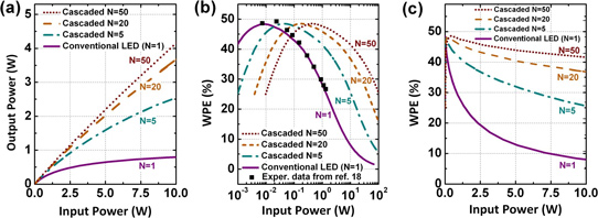
Figure 2: Change in (a) output power, (b) wall-plug efficiency (WPE) on logarithmic scale (c), and WPE on linear scale of modeled reference single-junction LED and cascaded LEDs with various cascade numbers (N). Experimental data and model fit for 470nm LED are also shown in (b).
Another benefit of cascading LEDs in this way was found to be reduced Joule heating, since the current through the layers was reduced to the level needed to avoid droop. By stacking up to 50 devices, the Joule heating effect could be reduced by more than an order magnitude, compared with single-active-region LEDs at the same output power. “This not only enhances efficiency but also can enable LED operation at elevated output power, and could eliminate thermal management issues,” the researchers write.
At this point, there are several challenges to overcome before this approach can be applied to LEDs: “First, GaN-based tunnel junctions based on MBE and metal-organic chemical vapor deposition (MOCVD) growth are still relatively less efficient than the results described here and reported previously using MBE growth. Another challenge is the activation of buried Mg-atoms (p-type dopant) in MOCVD/MOVPE growth, which has been addressed previously using sidewall activation. Finally, re-absorption of photons for LEDs with a large number of active regions, and excessive heating due to unextracted photons could both reduce the efficacy of these LEDs.”
LED efficiency droop LEDs MBE GaN substrates
http://link.aip.org/link/doi/10.1063/1.4819737
The author Mike Cooke is a freelance technology journalist who has worked in the semiconductor and advanced technology sectors since 1997.
