- News
22 August 2013
Exploring graded electron-blocking layers for nitride LEDs
Researchers in South Korea and USA have been developing graded-composition superlattice electron-blocking layers (GSL-EBLs) for nitride semiconductor light-emitting diodes (LEDs) [Jun Hyuk Park et al, Appl. Phys. Lett., vol103, p061104 2013]. The team consisted of scientists/engineers from Pohang University of Science and Technology (POSTECH), Rensselaer Polytechnic Institute (RPI), Seoul Opto-device Co, and Chonbuk National University.
Electron-blocking layers are used to confine electrons to gallium indium nitride (GaInN) multiple quantum well (MQW) active regions in attempts to improve efficiency. Electrons in nitride semiconductor LEDs can overshoot the light-emitting region, ending up in the p-contact and recombining non-radiatively with holes, reducing efficiency and hole injection into the MQW. Up to now, using EBLs to reduce these effects has had mixed results. Such structures often do not reduce overshoot as expected. At the same time, the EBL also tends to create a barrier to the injection of holes into the MQW.
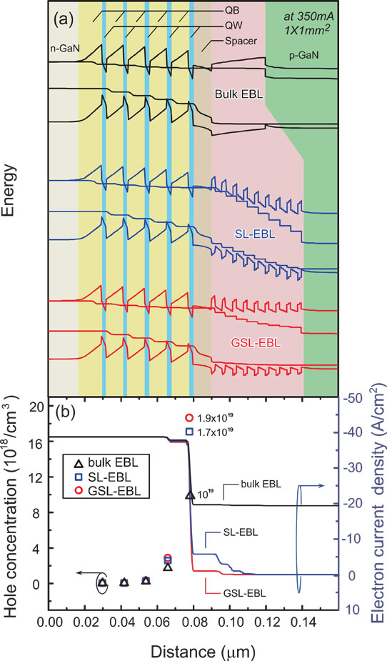
The researchers designed their test EBL structures by performing a series of Advance Physical Model of Semiconductor Devices (APSYS) simulations (Figure 1). They found that using a superlattice structure with graded aluminium gallium nitride (AlGaN) layers and gallium nitride (GaN) bilayers reduced electron overshoot and improved hole injection. The grading of the AlGaN was also designed to avoid a penalty in operating voltage that arises in ungraded SL structures.

Figure 1: (a) Energy band diagrams and (b) hole concentration and electron leakage current of GaInN/GaN MQW LEDs with three different EBL structures at 350mA injection current, as calculated by APSYS simulator.
Actual LED structures were grown on c-plane sapphire substrates by metal-organic vapor phase epitaxy (MOVPE). The buffer was 2μm of GaN. This was followed by a short-period GaInN/GaN superlattice with 20 periods, 3μm of n-GaN, a quantum well (MQW) active region, the EBL, and a 100nm p-GaN contact. The MQW was a five-period structure with 9nm GaN barriers separating 3nm Ga0.8In0.2N wells.
Three types of EBL were implemented: an 18nm p-Al0.2Ga0.8N bulk material; a five-period GSL-EBL with p-AlxGa1-xN/p-GaN 2nm/3.6nm bilayers graded from x values of 0.23 to 0.07 from the MQW to the p-GaN contact; and a nine-period GSL-EBL with 2nm/2nm bilayers where the x values grade over the same range as in the five-period structure.
The LED wafers were processed into 600μm x 600μm mesa-type devices. The n-contact was annealed titanium/aluminium and the p-contact was annealed indium tin oxide transparent conductor with chromium/gold metal pads.
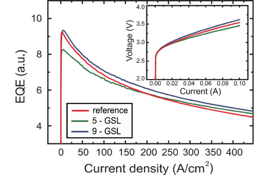
The light output power (L), current (I) and voltage (V) performance of the devices was measured and the external quantum efficiency (EQE) was extracted (Figure 2). The nine-period GSL-EBL showed slightly improved peak efficiency and reduced droop effect over the bulk EBL. The droop at 100mA was 7.8% for the nine-period GSL-EBL compared with 9.7% for the bulk EBL. The efficiency droop was even less apparent in the five-period GSL-EBL at 5.6%, but at the cost of lower peak efficiency.

Figure 2: EQE as a function of injection current for GaInN LEDs with three different EBL structures. Inset: I-V characteristics.
The 20mA forward voltages for the devices were 3.00V for the bulk EBL, 3.05V for the nine-period GSL-EBL, and 2.95V for the five-period GSL-EBL. It is thought that the increased voltage for the nine-period GSL-EBL is due to its increased thickness, leading to increased resistance to current flow. Higher forward voltages indicate a source of power loss.
Temperature-dependent measurements suggested that the problem with the 5-period EBL was related to “somewhat inferior” crystal quality compared with the other devices. The poor quality increased Shockley-Read-Hall recombination through defect levels at low current, reducing the peak efficiency. At current densities above 200A/cm2, where SRH recombination becomes less significant, the five-period EBL performed better than the bulk EBL in terms of EQE.
The researchers comment: “We anticipate that GSL-EBL LEDs optimized in terms of crystal quality and structure will show not only a higher efficiency with reduced droop but also an even lower operating voltage than LEDs with conventional bulk EBL.”
http://link.aip.org/link/doi/10.1063/1.4817800
The author Mike Cooke is a freelance technology journalist who has worked in the semiconductor and advanced technology sectors since 1997.


