


- News
26 December 2013
MOCVD surface roughening for photon absorption boost in InGaN solar cell
Researchers at University of California Santa Barbara (UCSB) have used low-temperature metal-organic chemical vapor deposition (MOCVD) of p-type gallium nitride (GaN) to achieve intentional surface roughening of a solar cell device, thereby increasing photon absorption and boosting performance [R. M. Farrell et al, Appl. Phys. Lett., vol103, p241104, 2013]. Funding for the work came from US Defense Advanced Research Projects Agency (DARPA) High Performance InGaN-Based Solar Cells Program, the California Advanced Solar Technologies Institute, and the US Solid State Lighting and Energy Center (SSLEC).
The absorbing layer of the device (Figure 1) consisted of intrinsic indium gallium nitride (InGaN). It is hoped to develop such solar cells that convert shorter-wavelength photons from the sun as part of a photovoltaic system where different wavelength bands are separated for efficient-energy conversion by suitable devices.
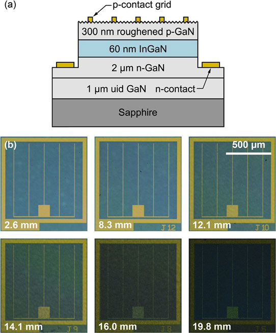
Figure 1: (a) Cross-sectional schematic of device structure. (b) Optical micrographs of fabricated solar cells at six different positions along radius of sample.
The UCSB nitride semiconductor photovoltaic (PV) device could be used to extend the 44% conversion efficiency achieved by GaInP/GaAs/GaInNAs multi-junction cells, hopefully to beyond 50%. However, because of the surface roughening needed to improve the nitride semiconductor photon absoption, the UCSB technique is not really suitable for a stacked multi-junction PV format.
The UCSB team also believes that the surface roughening technique could be used in the other direction to improve light extraction efficiency of InGaN-based light-emitting diodes.
The p-type/intrinsic/n-type (p-i-n) epitaxial layers of nitride semiconductor for the solar cell were grown by MOCVD on 50mm (0001) sapphire. The surface roughening of the p-GaN layer was achieved by relatively fast growth at low temperature. The roughness increased toward the edges of the wafer due to temperature variation in the reaction chamber. The roughened surface was faceted with a high density of V-defects.
The increasing roughness along the radius of the sample reduces the reflectivity of the surfaces, as seen in the optical micrographs of Figure 1b. Atomic force microscopy (AFM) showed an increase in root mean square (RMS) roughness from around 7nm to 36nm. The largest value for roughness came around 20mm along the radius of the sample, after which it declined slightly.
The solar cells were fabricated using standard processes. The 1mm x 1mm mesas were created using dry etching. The p-contacts consisted of palladium/gold applied in a grid pattern. The n-contact was a ring of aluminium/gold at the base of the mesa.
The increased roughness leads to increased external quantum efficiency (EQE) and short-circuit current (Figure 2). At 3.8mm radial position the peak EQE (at about 380nm wavelength) was 61.0% – this increased to 77.5% (+27.1%) at 21.7mm. The long-wavelength absorption edge also shifted with radial position – from ~430nm at 3.8mm to ~450nm at 21.7mm. The improved absorption of longer wavelengths is attributed to an increased indium content of the InGaN layer. At the high growth temperatures typically used for p-GaN growth the indium of the InGaN layer tends to dissociate, reducing the concentration.
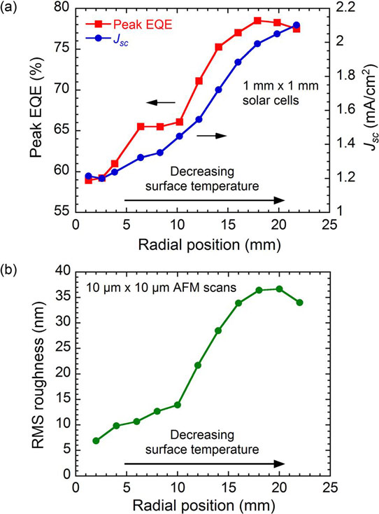
Figure 2: (a) Dependence of peak EQE and short-circuit current density (Jsc) on radial position. (b) Dependence of RMS roughness on radial position.
The short-circuit current was measured under AM1.5G illumination. At 3.8mm radial position the short-circuit current density was 1.24mA/cm2. At 21.7mm this was increased by 69.4% to 2.10mA/cm2. The increase is attributed to both the improve peak EQE and the shift of the absorption edge to longer wavelengths.
On the other hand, the open-circuit voltage is reduced by increasing surface roughness, being 1.93V at 3.8mm and 1.54V at 21.7mm. This effect is related to an increase in dark current and current leakage caused by the V-defects. The researchers point out that more advanced device designs are available to ameliorate this effect where the p-GaN is applied in a series of layers to avoid the V-defects extending down to the active InGaN layer.
http://dx.doi.org/10.1063/1.4844955
The author Mike Cooke is a freelance technology journalist who has worked in the semiconductor and advanced technology sectors since 1997.


