


- News
13 December 2013
Vertical spacers for tighter integration of III-V MOSFETs
University of California Santa Barbara (UCSB) researchers have been studying the effect of using undoped vertical spacers in the source and drain contacts to reduce off-state leakage in indium arsenide (InAs)-channel metal-oxide-semiconductor field-effect transistors (MOSFETs) [Sanghoon Lee et al, Appl. Phys. Lett., vol103, p233503, 2013]. The team used the technique to achieve the highest peak transconductance value for any III-V MOSFET to date.
III-V MOSFETs are being developed with a view to high performance in very large-scale integration (VLSI) ICs. Although some promising results have been reported, the devices tend to be larger than desired due to the need to reduce leakage currents in the off-state. In particular, the source and drain contacts are difficult to shrink or to move closer to the gate edge. One reason for this is the need to reduce the size of the electric fields that cause leakage at high drain bias. The UCSB vertical spacers are designed to reduce these fields without increasing source-drain distances.
Solid-source molecular beam epitaxy (SS-MBE) on indium phosphide (InP) substrates was used to create samples for three device types (Figure 1). Under the channel was a series of indium aluminium arsenide (InAlAs) layers: a 50nm unintentionally doped buffer, a 250nm p-type barrier, a 2nm pulse-doped n-type region, and a 5nm unintentionally doped setback. The transistor layers consisted of a 3nm indium gallium arsenide (In0.53Ga0.47As) sub-channel, 6nm InAs strained channel, and 3nm In0.53Ga0.47As upper cladding. The structure was capped with 5nm of In0.53Ga0.47As, which was doped n-type in one case (sample A) and undoped in two cases (samples B and C).
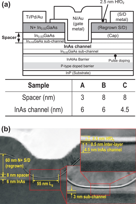
Figure 1: (a) Schematic cross-section of device structure. Table defines differences between three experimental samples. (b) High-angle annular dark field (HAADF) scanning transmission electron microscopy (STEM) cross-sections of 55nm-gate-length device based on sample C.
The source/drain regions were created by first forming a dummy gate of patterned 150nm spin-on hydrogen silsesquioxane (HSQ) and then selective re-growth of 60nm of heavily n-type In0.53Ga0.47As using metal-organic chemical vapor deposition (MOCVD).
Transistor fabrication started with mesa isolation and dummy gate removal using a buffered oxide etch. Digital etch of the gate region removed all of the cap and some or all of the upper cladding. In sample C, the digital etch continued 1.5nm into the InAs channel.
The processing continued in an atomic layer deposition (ALD) system, where the samples were cleaned and passivated before depositing hafnium dioxide as a gate insulator. The devices were then annealed at 400°C for 15 minutes in forming gas (5% hydrogen, 95% nitrogen). Nickel/gold was used for the gate electrode. The source/drain electrodes were titanium/palladium/gold.
In two 75nm-gate-length devices based on samples A and B, the increased spacer height of 8nm (compared with 3nm) reduced off-state leakage five-fold at a gate potential of -0.3V and drain bias of 0.5V. The peak transconductances (gm) of devices A and B were roughly the same over the range of gate lengths 60nm to 1μm. The peak gm with a 60nm gate was 2.7mS/μm, which the researchers claim as a record “in any III-V MOSFET technology to date”. The increased spacer height of sample B also reduced, and hence improved, the subthreshold swing (SS) by 10-15% over the same gate length range. At 60nm gate length, SS was 125mV/dec.
Although the on-resistance extrapolated to zero gate length was slightly higher in sample B (190Ω-μm, compared with 181Ω-μm for sample A), the discrepancy was within fitting error, according to the researchers.
The effect of bringing the gate closer to the channel in sample C devices was to reduce peak gm by about 10%, while improving SS (Figure 2). The better SS is attributed to the better electrostatic control of the gate and the larger bandgap arising from the quantum confinement of the channel (~0.50eV compared with ~0.44eV, according to Schrödinger-Poisson modeling). The reduced gm is possibly due to surface roughness scattering effects.
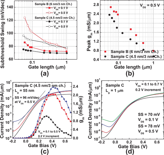
Figure 2: (a) Subthreshold swing versus gate length (Lg), at 100mV and 500mV drain bias (VDS), for samples B and C. (b) Peak transconductance verus Lg, at 500mV VDS, for samples B and C. (c) Drain current versus gate potential and transconductance of sample C at 55nm Lg. (d) Drain current versus gate potential of sample C at 1μm Lg.
A 55nm-gate sample C transistor had an SS of 96mV/dec and gm of 2.4mS/μm at 0.5V drain bias. With a 1μA/μm drain current threshold, the voltage was 60mV and the drain-induced barrier lowering (DIBL) was 130mV/V. A 1μm gate length with sample C reduced SS to 70mV/dec. This value gives an estimate for the interface trap density of 5x10¹²/cm2-eV.
MOSFETs InAs InAs MOSFETs InP substrates SS-MBE MOCVD ALD
http://dx.doi.org/10.1063/1.4838660
The author Mike Cooke is a freelance technology journalist who has worked in the semiconductor and advanced technology sectors since 1997.


