

- News
7 February 2013
New atomic layer deposition process for nitride LED reflector structures
Researchers in China have developed an atomic layer deposition (ALD) technique to create distributed Bragg reflectors (DBR) for increasing nitride semiconductor light-emitting diode (LED) output power by up to 43% [Hongjun Chen et al, Appl. Phys. Express, vol6, p022101, 2013].
Although some groups have developed DBRs for such purposes before, this is claimed as the first proposal and demonstration of DBRs grown using ALD rather than electron-beam (EB) evaporation. The advantages of ALD over EB evaporation include better thickness uniformity over large-diameter substrates and thickness control at the atomic level.
To develop an ALD process, the researchers from Institute of Microelectronics of Chinese Academy of Sciences and Southeast University changed the composition of the DBR from the usual titanium dioxide (TiO2) and silicon dioxide (SiO2) pairs to a titanium dioxide and aluminium oxide (Al2O3) recipe. The use of Al2O3 also allows better adhesion of Al metal so that Al-mirror/DBR combinations can be developed. With TiO2/SiO2 DBRs, an extra layer of Al2O3 is often applied to enable adhesion of Al-metal.
The LED structure (Figure 1) was grown on a patterned sapphire substrate (PSS) by metal-organic chemical vapor deposition (MOCVD). PSS has two effects: improved crystal quality and light extraction. These effects increase the number of photons generated in the active region and their ability to exit the device, respectively.
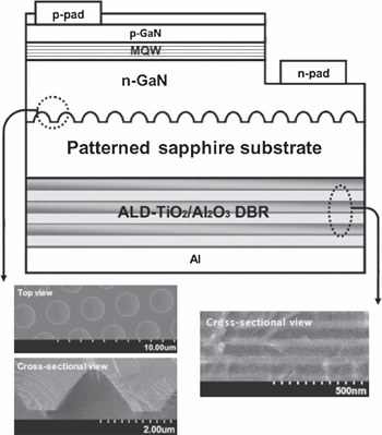 Figure 1: Schematic diagram of LED with backside reflector composed of TiO2/Al2O3 DBR and Al mirror grown on backside of PSS. Insets: SEM images of fabricated DBR and PSS.
The sapphire patterning was achieved using photolithography and inductively coupled plasma reactive ion etch (ICP-RIE). The diameter and spacing of the bumps were 2.1μm and 900nm, respectively. The pattern height was ~1.3μm.
The nitride heterostructure consisted of a 30nm GaN buffer, 4.5μm n-type GaN contact/buffer, 6-period InGaN/GaN multi-quantum well (MQW), and 0.9μm p-GaN contact. A 240nm indium tin oxide (ITO) transparent contact layer was also applied. The metal electrodes for the p- and n-contacts consisted of chromium/platinum/gold. Silicon dioxide was also used as a 100nm passivation layer.
The LED wafer was back-side thinned to 100μm before the DBR and Al mirror were applied. The atomic layer deposition was preceded by soft polishing for 30 minutes to minimize the roughness of the surface. The TiO2/Al2O3 DBR was designed to maximize reflectivity between 420nm and 500nm. This was achieved with 67nm Al2O3 and 49nm TiO2.
The ALD used trimethyl-aluminium and water precursors for the Al2O3, and titanium tetrachloride and water for the TiO2. The carrier gas was nitrogen. The growth temperature for both materials was 250°C. This enabled a reduced fabrication time and high-quality thin films. The different material depositions were separated by nitrogen purging to avoid mixing of the respective precursors.
The DBR was capped with 150nm of aluminium deposited using electon-beam evaporation. Devices with TiO2/SiO2 (48.5nm/78.5nm) DBRs deposited using electron-beam evaporation were also produced. These were finished with a 15nm Al2O3 adhesive layer and 150nm Al metal.
The LED chips measured 300μm x 700μm, defined using laser scribing and singulation. The breaking process of the singulation was found to cause some lift-off of the aluminium from TiO2/SiO2 DBR but not in the case of the new TiO2/Al2O3 DBR.
Although DBRs without Al mirror did reflect some light, it was found that the reflectivity became more effective (~95% reflectivity) and nearly independent of wavelength and incident angle with the Al mirror.
Six device types were fabricated on patterned sapphire and one on flat sapphire. The devices on patterned sapphire showed almost identical electrical performance with 3.05V forward voltage at 60mA current injection.
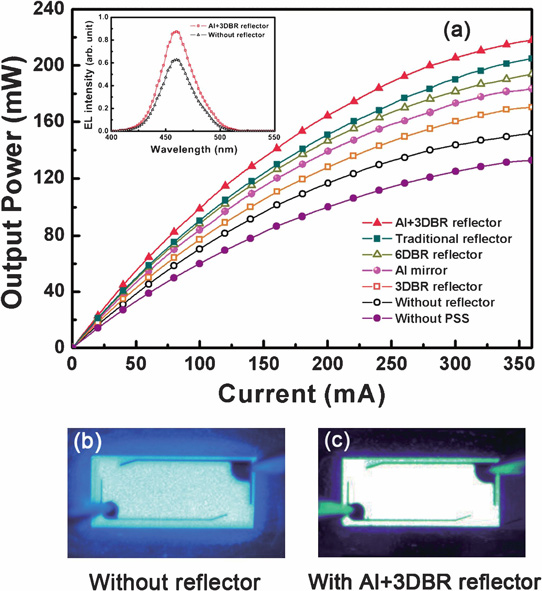
Figure 2: (a) LOP of fabricated LEDs versus injection current. Inset: electroluminescence spectra. (b) and (c) are photographs of LEDs with and without backside reflector in operating state, respectively.
The light output power (LOP, Figure 2) was greatest for an LED with Al-mirror and 3-pair TiO2/Al2O3 DBR (Al+3DBR). At 60mA injection the LOP for the Al+3DBR LED was 65mW, compared with 58.7mW for a conventional 3-pair TiO2/SiO2 DBR reflector, 57.4mW for 6DBR-only, 54.6mW for Al-only, 50mW for 3DBR-only, 45.4mW no-reflector, and 39mW for the device grown on flat sapphire. The light output improvement for the best device was 43.1% over that for the LED with no reflector. The peak wavelength was ~460nm.
The improvement over the traditional reflector structure was attributed to the better uniformity and thickness control of ALD compared with EB evaporation.
http://apex.jsap.jp/link?APEX/6/022101
The author Mike Cooke is a freelance technology journalist who has worked in the semiconductor and advanced technology sectors since 1997.
