

- News
25 February 2013
Direct growth of InGaN on silicon
Researchers in Spain have grown high-indium-content indium gallium nitride (InGaN) directly on silicon (Si) substrates [Praveen Kumar et al, Appl. Phys. Express, vol6, p035501, 2013]. The work was carried out at Universidad Politécnica de Madrid’s Institute for Systems based on Optoelectronics and Microtechnology (ISOM).
InGaN is an important optoelectronic material capable of producing longer-wavelength light-emitting diodes and laser diodes than other nitride semiconductor materials. The energy bandgap can be varied in the range from infrared through visible light to near-ultraviolet. The material is also of interest in energy conversion/solar cells.
However, InGaN is challenging to grow, particularly at higher indium fractions. Among the difficulties is a tendency for phase separation where regions of InGaN with different indium concentrations form. Further problems arise from InN decomposition and In desorption that reduces In content.
Generally, InGaN is grown at lower temperature than pure GaN to avoid some of these problems. Previously, direct growth of InGaN on silicon has been considered impossible, and instead aluminium nitride/gallium nitride buffer layers are usually grown first. The junction of InGaN/GaN/AlN/Si isolates the InGaN layer from the substrate. One would like an ohmic junction between InGaN and silicon devices in tandem solar cells. In fact, the In0.46Ga0.54N/Si junction has been theoretically predicted to be ohmic due a unique band alignment effect.
The InGaN was grown directly on p-type Si (111) substrates using plasma-assisted molecular beam epitaxy (PAMBE) on a MECA 2000 system. The growth was preceded by native oxide removal at 800°C and annealing at 850°C for 20 minutes. The silicon surface was then exposed to active nitrogen for 5 minutes at 850°C, leaving a layer of silicon nitride. Such a nitride preparation was developed previously for GaN PAMBE on Si (111) by Japan-based researchers in 1998.
The InGaN growth was carried out using an indium flux of 4.2nm/min and a gallium flux of 4.6nm/min. The nitrogen flux was varied from slightly above ‘stoichimetry’ at 9.2nm/min (i.e. > (4.2 + 4.6)nm/min) until columnar growth conditions were achieved. The InGaN growth rate was 0.45μm/hour. The target layer thickness was 450nm. Various growth temperatures were tried (Figure 1).
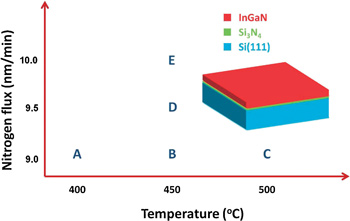 Figure 1: Diagram of the growth conditions of the InGaN layers A–E. Inset: scheme of the sample structure.
Sample B gave the best structure for device applications (Figure 2). The other samples suffered from nanoscale flake, network, hole, or dot-like structures. By contrast, sample B has laterally extended, micrometer-sized planar areas together with trenches and holes. In particular, macroscopic planar regions of sample B have a very smooth root-mean-square roughness of only 1.7nm in atomic force microscopy (AFM) measurements.
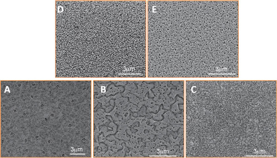
Figure 2: Top-view SEM images of InGaN layers A–E grown directly on Si.
The researchers comment on the macroscopic planar regions that they are connected to each other and are large enough to serve as barrier layers for active structures such as quantum wells and quantum dots.
The absence of In or Ga droplets on the surface is taken as an indication that all the In is incorporated into the layer. The target In composition was 40-50%. The researchers believe that there is no InN decomposition and the growth temperature is considered too low for In desorption.
X-ray analysis of the GaN(0002) reflection peak indicates InGaN layers fluctuating between 45% and pure GaN for all samples except B. The low-growth-temperature sample A has no x-ray reflection peak, suggesting amorphous InGaN. In sample B, instead of a broad peak, there are two narrower peaks for regions of GaN (17.26°) and InGaN (16.59°). The half-width of the GaN peak is 0.14°. The InGaN peak width suggests In compositions between 38 and 45%.
The researchers comment: “The existence of these well-separated reflections is evidence for distinct, well-separated, and macroscopically extended regions of GaN plus low-In-composition InGaN and of InGaN with high and relatively uniform In composition. It is likely that the high-In-composition regions are the macroscopically extended planar layers, while the GaN plus low-In-composition regions are associated with the trenches and holes, exposing slow-growth planes to inhibit the incorporation of In.”
Photoluminescence (PL) of sample B at 12K had peaks at 358nm, 383nm and 794nm, associated with GaN, low-In-composition InGaN, and high-In-composition InGaN, respectively. According to the researchers, the long-wavelength peak would be associated with the energy gap of In0.41Ga0.59N. The long-wavelength peak is rather small due to the presence of defects. “However, the mere observation of PL opens space for further improvement of the optical quality,” the researchers write.
Current-voltage measurements of the junction between the n-type InGaN and p-type Si substrate were made by applying top and bottom aluminium contacts to the structure. The junction was perfectly ohmic between ‑3V (‑60mA) and +3V (+60mA). The n-type conduction of the InGaN layer is the result of native defects such as nitrogen vacancies in the crystal structure. The low-In-content InGaN/pure GaN trench and holes regions do not reach the silicon layer nor the top contact, so the conduction is due to the junction between high-In-content InGaN and Si substrate.
The silicon substrate is very high quality and the resistivity of the InGaN/Si structure is found to be almost the same as a bare silicon control sample.
The researchers comment that the comparison with the bare silicon measurement suggests that “no energy barrier is introduced by the SiN and, most importantly, proves that an ohmic contact is formed between the p-Si substrate and n-InGaN layer, confirming the theoretical prediction and consolidating the foundation for advanced device applications.”
The team concludes: “After having achieved this crucial step of the growth of macroscopically extended planar layers of InGaN with high In composition directly on Si, fine tuning of the growth parameters in the regime of low growth temperature and low active N flux is now straightforward to further improve the material quality.”
http://apex.jsap.jp/link?APEX/6/035501
The author Mike Cooke is a freelance technology journalist who has worked in the semiconductor and advanced technology sectors since 1997.
