

- News
20 February 2013
GaN FinFET without heterostructure
Researchers based in South Korea and France have developed gallium nitride (GaN) fin field-effect transistors (FinFETs) with the lowest claimed subthreshold swing for nitride semiconductor metal-insulator-semiconductor FETs (MISFETs) [Ki-Sik Im et al, IEEE Electron Device Letters, published online 30 January 2013].
The FinFET devices, produced by Kyungpook National University (South Korea), Grenoble Polytechnic Institute (France) and Samsung LED Company, are also the first to use heterostructure-free GaN. Usually, nitride semiconductor transistors use heterostructuring to create a two-dimensional electron gas (2DEG) near the junction between two or more different nitrides. The 2DEG serves as the channel conducting medium in these devices.
Some research groups, starting in 2009, have produced FinFETs using heterostructured nitride semiconductors, but the devices have suffered from parasitic conduction of the 2DEG. This creates problems for reliable operation due to poor GaN/gate oxide insulator interface quality.
The researchers see their device as a promising candidate for high-performance and high-speed integrated circuits, and also for high-power applications since GaN semiconductor is able to withstand stronger electric fields than silicon and most other semiconductor materials.
The epitaxy for the GaN FinFET (Figure 1) consisted of a simple 120nm n-type (silicon-doped) GaN metal-organic chemical vapor deposition (MOCVD) layer on a GaN/sapphire template. The Hall carrier density and mobility were 1x10¹⁸/cm3 and 234cm2/V-s, respectively. The fin channel was patterned with electron-beam lithography and plasma reactive-ion etching. The plasma damage was repaired using tetramethyl ammonium hydroxide solution to create smooth surfaces. The height and width of the fin were 120nm and in the range 40-120nm, respectively.
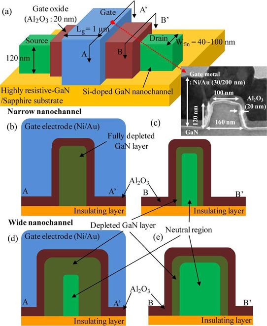
Figure 1: (a) Schematic illustration of GaN nanochannel FinFET including device dimensions. (b) and (c) Narrow fin: The (dark green) depletion region extends across whole body (full depletion) in OFF state and gradually reduces with increasing gate bias. (d) and (e) Wide fin: Body cannot be fully depleted. Inset: cross-sectional TEM image.
The maximum drain current of a 5-finger FinFET with nanochannels of 60nm width and 1μm length was more than 1mA (Figure 2). The peak transconductance of 0.25mS occurred at 6V gate and 7V drain. Normalizing according to the effective gate width (5x(120nm+60nm+120nm) = 1.5μm) gives a maximum drain current density of 670mA/mm and a peak transconductance of 168mS/mm.
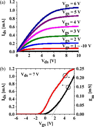 Figure 2: (a) Drain current and voltage characteristics of GaN FinFET with 1μm gate length, 60nm fin width, and five parallel fins. (b) Transfer curves of drain current and transconductance with gate voltage at 7V drain.
The researchers comment that these results are higher than those of state-of-the-art planar-type AlGaN/GaN-based normally-off (enhancement-mode) MISFETs and MISHFETs.
The off-state current for devices with channel widths less than 100nm were as low as 10-11mA due to the total depletion of the fin below threshold. The on/off current ratio was 108.
A device using 60nm-wide fins had a subthreshold swing (SS) of 68mV/dec, the lowest value ever reported for GaN MISFETs, according to the researchers, and close to the theoretical limit of 60mV/dec for planar devices. Lower values of SS can be reached with tunnel-junction devices.
The researchers suggest that the junctionless/heterostructure-free architecture reduces the effect of interface traps, but they also point out that the effect on subthreshold swing of such structures is the subject of controversy in the research community.
With a 1μm gate-length and 2μm gate-drain underlap, the off-state (-3V gate) breakdown voltage was ~280V. The researchers believe that the breakdown point could be increased with longer gates, but at the price of lower on-current. Field-plates and gate recessing are other strategies that could increase breakdown voltages.
Gate leakage at -13V gate potential was only 10-12A, despite the extremely thin 20nm Al2O3 gate insulation.
The author Mike Cooke is a freelance technology journalist who has worked in the semiconductor and advanced technology sectors since 1997.
