

- News
12 February 2013
Etch stop structure opens up gate recess improvement for GaN MISFET
A team at Massachusetts Institute of Technology has developed an etch stop technique to improve performance of recessed-gate nitride semiconductor metal-insulator-semiconductor field-effect transistors (MISFETs) [Bin Lu et al, IEEE Electron Device Letters, published online 24 January 2013].
Recessing involves etching the top barrier layers of nitride heterostructure FETs to bring the gate closer to the two-dimensional electron gas (2DEG) channel. This increases the electrostatic control and also tends to shift the threshold voltage from negative to positive values. Positive thresholds give normally-off/enhancement-mode operation for the transistor. Normally-off operation is preferred for fail-safe power switching and low-power consumption.
However, recessing usually involves plasma etching that damages the semiconductor heterostructure, reducing performance. In particular, plasma damage creates a high density of defect states, degrading the channel mobility in the recessed region. This increases on-resistance.
Another problem is that the etch process is difficult to control, creating unpredictable device performance. This becomes even worse when different recessing is needed in devices being fabricated at the same time because the etch process proceeds at different rates according to the aspect ratio of the recessed region.
The MIT researchers have developed the new barrier structure to enable them to overcome these problems, significantly improving performance.
The epitaxial structure (Figure 1a inset) was grown on 4-inch (111) p-type silicon using metal-organic chemical vapor deposition (MOCVD). The top n-type gallium nitride (GaN) layer was doped with silicon at a concentration of 3-6x10¹⁸/cm3. The effect of the doping is to deplete the maximum electron density in the n-GaN to less than 1016/cm3 (Figure 1a).
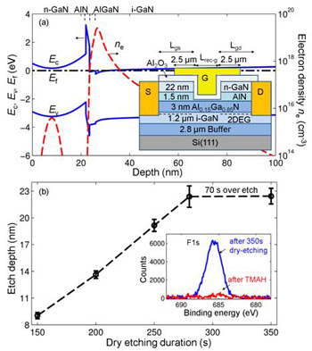 Figure 1: (a) Band structure and electron density profile of MIT wafer structure. Inset shows relevant dimensions of recessed-gate GaN MISFET. (b) Recess depth as a function of etch duration. Inset: XPS F1s signal of sample dry-etched for 350 seconds and subsequently wet-etched by TMAH.
The 2DEG characteristics are sheet resistance 580Ω/square, electron mobility 1530cm2/V-s, and sheet charge density 7x10¹²/cm2.
Devices were isolated from each other through mesa etching. The ohmic metal electrodes for the source-drain contacts consisted of titanium/aluminium/nickel/gold.
The gate recess etch used the selectivity for n-GaN over AlN of a fluorine-based electron-cyclotron-resonance reactive ion etching (ECR-RIE). The selectivity arises from the non-volatility of aluminium fluoride (AlF3). The etch gas recipe consisted of 5 standard cubic centimeters per minute (sccm) of boron trichloride and 35sccm of sulfur hexafluoride at 35mtorr. The etch time of 350 seconds was found to completely remove the n-GaN layer (Figure 1b). A further 70 seconds of over-etch time was added.
The dry etch damage was repaired by first oxidizing the exposed AlN and wet etching in tetramethylammonium hydroxide (TMAH) at room temperature for 1 minute. X-ray photoelectron spectroscopy (XPS) analysis showed much reduced fluorine at the AlN surface after the treatment (Figure 1b inset).
The AlN surface was further cleaned with ultraviolet-ozone and hydrochloric acid before atomic layer deposition (ALD) and annealing of aluminium oxide dielectric as gate insulation. The T-gate metal electrode consisted of nickel/gold. Finally a further annealing step was then carried out to reduce the positive fixed charge that can arise in aluminium oxide.
The threshold voltage of a 3μm gate device was positive, at +0.3V, indicating normally-off enhancement-mode operation (Figure 2).
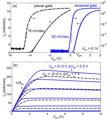 Figure 2: (a) Id-Vgs characteristics at Vds = 0.1V with bi-directional gate sweep; (b) Id-Vds characteristics. Recessed-gate transistor had Lrec-g = 3μm and Lgs = Lgd = 4μm. Planar-gate transistor (dashed line) has same Lsd with Lg = 8μm and Lgs = Lgd = 1.5μm.
The subthreshold swing was 62mV/dec, a value close to the 60mV/dec room-temperature limit for planar-gate devices. In fact, a comparison (i.e. non-recessed) planar-gate device had a somewhat higher swing of 76mV/dec.
The on-resistance of the devices was similar, at around 10Ω-mm, with a source-drain distance of 11μm. The maximum drain current was relatively low, the researchers write, “due to the large gate length and gate-to-source distance, relatively low 2DEG density (7.1×10¹²/cm2) and high contact resistance (1.2Ω-mm) of the non-optimized ohmic contact.”
The maximum effective mobility of the recessed device extracted from capacitance-voltage (CV) measurements was 1131cm2/V-s, somewhat lower than the Hall value of the 2DEG given above. However, the effective value is significantly better than other reported results on normally-off GaN MISFETs, according to the researchers.
Further CV measurements led the researchers to conclude: “The recessed-channel dielectric/semiconductor interface has very low interface state density, which results in small hysteresis and frequency dispersion in the CV measurements.”
Three-terminal breakdown was also measured at 50V for 0V gate, gate-length 3μm, gate-drain 12μm and drain leakage 68nA/mm.
This work was funded by the ARPA-E ADEPT and GIGA projects of US Department of Energy (DOE) and by the US Office of Naval Research.
http://ieeexplore.ieee.org/xpl/articleDetails.jsp
The author Mike Cooke is a freelance technology journalist who has worked in the semiconductor and advanced technology sectors since 1997.
