


- News
10 January 2013
InGaN-channel HEMT cut-off reaches 260GHz
Researchers at University of Notre Dame and Kopin Corp have developed high-performance nitride semiconductor high-electron-mobility transistors (HEMTs) with indium gallium nitride (InGaN) channels [Ronghua Wang et al, Appl. Phys. Express, vol6, p016503, 2013]. The performance of the devices is approaching that of GaN-channel HEMTs.
Incorporation of indium in GaN is expected to improve frequency performance in a similar way that indium gallium arsenide (InGaAs) is used to boost device speeds over pure-GaAs devices. The peak cut-off frequency for GaN HEMTs is presently more than 300GHz. The UND/Kopin InGaN device has a cut-off of 260GHz and a record-breaking square root of the product of the cut-off and maximum oscillation frequencies of 239GHz.
Although InGaN has a higher predicted steady-state drift velocity (highest with InN) than GaN (based on the lower electron effective mass), there are a number of factors that presently hinder real-world performance. For example, electron mobility is reduced due to alloy scattering effects. Further problems arise from the instability of InGaN during high-temperature growth, creating material inhomogeneity and rough interfaces that reduce electron response to electric fields.
The InAlGaN/InGaN barrier/channel heterostructure was grown using metal-organic chemical vapor deposition (MOCVD) on silicon carbide (SiC) substrates (Figure 1). The quaternary InAlGaN barrier was chosen over ternary InAlN with a view to the higher-mobility channel that can be obtained. The GaN buffer layer also acts as a back barrier that confines the electron channel, reducing short-channel effects.
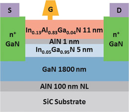
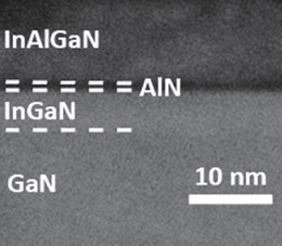
Figure 1: Schematic cross section of the InAlGaN/AlN/InGaN/GaN HEMT epitaxial layer structure with T-gates and non-alloyed MBE re-grown ohmic contacts, and cross-sectional STEM image confirming the InGaN channel thickness.
The n+-GaN source-drain regions were re-grown using molecular-beam epitaxy (MBE). The re-growth was followed by mesa isolation, ohmic metallization with titanium/gold, and nickel-gold T-gate formation using electron-beam lithography and lift-off. There was no passivation.
The resulting device had a contact resistance of 0.2Ω-mm. The channel had a sheet resistance of 264Ω/square, carrier density of 2.08x10¹³/cm2, and mobility of 1140cm2/V-second. The source-drain spacing was 1.6μm. The gate footprint was 50nm long and 2x25μm wide. The mushroom-head of the T-gate was 150nm.
The maximum current density of the device was 2.0A/mm at 1V gate potential. The researchers point out that the current performance is comparable with conventional quaternary-barrier InAlGaN HEMTs with GaN channels, since the channel charge density and mobility are similar. The on-resistance was 0.88Ω-mm. Three-terminal off-state breakdown occurred at ~15V with -8V gate bias (breakdown defined as off-current density exceeding 1mA/mm).
The peak extrinsic transconductance was 660-690mS/mm, achieved near pinch-off at around -4V gate bias. The threshold voltage was -4V at 0.1V drain and -4.4V at 6V (depletion-mode/normally-on). A comparable GaN-channel device produced and reported in 2012 by the UND/Kopin group had a threshold of -3.5V at 0.1V and -4.0V at 6.6V.
The researchers comment: “The more negative threshold voltage of the InGaN-channel HEMT is likely due to the slightly higher charge in the channel besides the inevitable variations in epitaxy and device fabrication.”
The frequency performance was measured between 100MHz and 110GHz. De-embedded values for the cut-off (fT) and maximum oscillation (fmax) frequencies were 260GHz and 220GHz, respectively (embedded values 140/186GHz). These results compare with a previous University of Illinois InGaN-channel HEMT (2004) with 0.18μm gate that had fT/fmax of 65/94GHz.
The geometric mean of the de-embedded values (square root of fT x fmax) was 239GHz, claimed as a record for InGaN-channel HEMTs. Increasing the mushroom-head of the T-gate is expected to increase the fmax/fT ratio.
The UND/Kopin work was supported partly by finance from the US Defense Advanced Research Projects Agency (DARPA), the US Air Force Office of Scientific Research, and the US Air Force Research Laboratory/Missile Defense Agency (AFRL/MDA).
Kopin InGaN HEMT SiC substrates MOCVD
http://apex.jsap.jp/link?APEX/6/016503
The author Mike Cooke is a freelance technology journalist who has worked in the semiconductor and advanced technology sectors since 1997.