

- News
22 January 2013
High-frequency InAs QW transistors for future system on chip and RF
Researchers from GLOBALFOUNDRIES, SEMATECH, and Massachusetts Institute of Technology (MIT) have extended their indium arsenide quantum well metal-oxide-semiconductor field-effect transistor (InAs QW MOSFET) technology to some of the highest and most balanced frequency performance yet seen [Dae-Hyun Kim et al, IEEE Electron Device Letters, published online 4 January 2013]. Many of the improvements in the latest work are attributed to the dramatically higher quality interface between dielectrics and III-V semiconductors enabled by atomic layer deposition (ALD) techniques developed in the last few years.
The device material was grown on an indium phosphide (InP) substrate (Figure 1). The structure featured a 300nm indium aluminium arsenide (In0.52Al0.48As) back barrier/buffer, silicon delta-doping, a 5nm InAlAs spacer, a 10nm channel, a 2nm InP etch stop, and a 10nm indium gallium arsenide (In0.53Ga0.47As) cap. The channel consisted of an InGaAs/InAs/InGaAs sandwich. The structure had a room-temperature Hall mobility of 8000cm2/V-s and sheet carrier density of 1x10¹²/cm2.
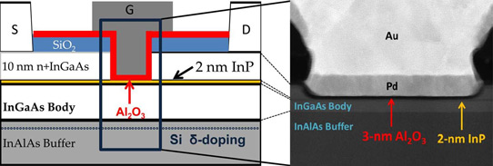
Figure 1: (Left) Device schematic and (right) transmission electron micrograph (TEM) image for the cross section of 100nm InAs MOSFETs with 3nm Al2O3.
Transistor formation consisted of mesa isolation, molybdenum/titanium/molybdenum/gold ohmic source-drain, silicon dioxide (SiO2) plasma-enhanced chemical vapor deposition (PECVD), electron-beam lithographic patterning and plasma/wet etch of the gate recess, atomic layer deposition of the 3nm aluminium oxide (Al2O3) gate insulator, and deposition of a palladium/gold gate electrode.
A 100nm-gate-length device demonstrated a positive threshold of 0.2V for 1μA/μm drain current at 0.5V drain bias. A positive threshold is desired for low-power-consumption enhancement-mode/normally-off transistors. The subthreshold swing was relatively low, at 105mV/dec, and the drain-induced barrier lowering was 100mV/V. These values are described as “excellent” in the research paper.
The gate leakage was suppressed to less than 1nA/μm at all measured biases by the Al2O3 insulation. The is a factor of 105 better than the forward bias values typical of III-V high-electron-mobility transistors (HEMTs) that depend on metal-semiconductor Schottky barriers to isolate the gate electrode.
The on-resistance for the InAs QW MOSFET at 0.8V gate potential was 370Ω-μm. The researchers comment: “This outstanding RON contributes to the maximum transconductance (gm,max) = 1720μS/μm at VDS = 0.5V.”
The frequency dependence of the devices was tested between 0.5GHz and 50GHz. The cut-off frequency (fT) of a 100nm-gate device of width 2x20μm was 248GHz. The maximum oscillation (fmax) was 302GHz. The researchers write: “To the knowledge of the authors, these are the best combination of fT and fmax at VDS = 0.5V, ever reported in any III–V MOSFET technology, and approach to advanced III–V HEMTs with similar gate lengths.”
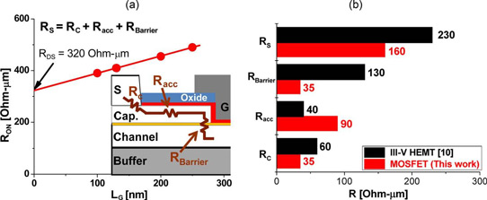
Figure 2: (a) RON as a function of Lg for InAs MOSFETs and (inset) simple model for Rs and (b) extracted components for Rs which arise from transmission line method (TLM) and RON analysis.
The researcher concluded with an analysis of the source resistance (Rs) obtained by comparing devices with different gate lengths (Lg). The team used a model that decomposed Rs into three terms: contact resistance (Rc) between the non-alloyed ohmic metal electrode and n+-GaN semiconductor, access resistance (Racc) between the ohmic and gate regions, and, finally the resistance of the InP etch stop barrier (RBarrier). The researchers believe the dominant component is Racc, which was estimated to be around 56% of the total (Figure 2). The application of a self-aligned ohmic contact process design is expected to significantly reduce the source resistance in the future.
InAs QW MOSFET InP substrate ALD
http://ieeexplore.ieee.org/xpl/articleDetails.jsp?tp=&arnumber=6403503
The author Mike Cooke is a freelance technology journalist who has worked in the semiconductor and advanced technology sectors since 1997.
