

- News
17 January 2013
Hafnium dioxide for gate insulation and surface passivation in nitride HEMTs
Seoul National University and Korea Electronics Technology Institute have been developing hafnium dioxide (HfO2) as a gate insulator for aluminium gallium nitride (AlGaN) metal-oxide-semiconductor high-electron-mobility transistors (MOSHEMTs) [Ogyun Seok et al, Semicond. Sci. Technol., vol28, p025001, 2013]. The researchers found that HfO2 has superior blocking characteristics, surface passivation properties and causes a smaller shift of threshold voltage compared with alternatives. A further attraction is that it has been demonstrated “for the first time” that the material can be deposited using simple RF-sputtering.
The nitride semiconductor layers were grown on (111) silicon substrates using metal-organic chemical vapor deposition (Figure 1). The buffer was carbon-doped to increase its resistivity. The structure resulted in a channel with electron mobility of 1740cm2/V-s, sheet carrier density of 6.81x10¹²/cm2, and sheet resistance of 528Ω/square.
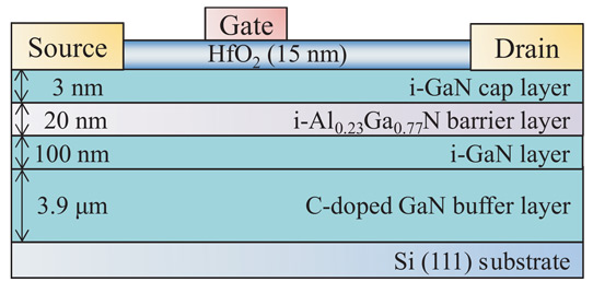
Figure 1: Cross-sectional view of AlGaN/GaN MOS-HEMT with HfO2 gate insulator.
The transistors were formed with mesa isolation, titanium/aluminium/nickel/gold ohmic source/drain electrodes, RF-sputtered HfO2 gate insulation, and nickel/gold Schottky gate. The sputtering was performed at low power and at room temperature under an argon gas flow. The aim of using low-power sputtering was to minimize damage to the underlying nitride semiconductor materials. The sputtering was preceded with a buffered oxide etch to remove any native oxide. The resulting HfO2 is found by x-ray analysis to be weakly crystalline.
The effect of the HfO2 insulator was to reduce the gate leakage to -67pA/mm at -10V gate-source potential and 100V drain bias, compared with -47μA/mm for a conventional HEMT without insulator. The reduction is some six orders of magnitude. The drain leakage under the same ‘off-state’ conditions was also not degraded by 100s of sustained DC stress, while for the conventional device the leakage increased from 57.5μA/mm to 496μA/mm.
The devices had 3μm gate-length and gate-source distance, and 20μm gate-drain distance. The researchers attribute the improved leakage performance for the transistor with HfO2 to the effective suppression of surface trap states for electrons from the gate electrode.
The HfO2 also blocked leakage under a forward gate-drain bias of +3V with a gate current of 11nA/mm, while the conventional device current was 56mA/mm. The leakage under a reverse bias of -10V was -33pA/mm for the MOSHEMT and -9.7μA/mm for the HEMT. The HfO2 continues to block current up to +10V, after which the gate current quickly rises to around 1000A/mm.
Further tests indicated that the HfO2 layer also has a passivating effect on the GaN surface layer, reducing surface leakage currents and electron trapping effects.
The researchers measured a three-terminal breakdown voltage (BV, when leakage current reaches 1mA/mm at a gate-source potential of -10V) of 1524V for the MOSHEMT (470V for the HEMT). The breakdown mechanism for the HEMT was electron runaway current from the gate through surface states.
The researchers comment: “In the proposed MOS-HEMT, the trap-assisted Schottky tunneling current and the surface leakage current caused by electron trapping are successfully suppressed by the HfO2 gate insulator such that the device with HfO2 sustains a high breakdown voltage.”
Another common problem with HEMTs is current collapse under pulsed gate and drain biases. The researchers found some amelioration of this in their MOSHEMTs, which they attribute to suppression of surface traps by the HfO2 layer.
The on/off ratio was determined using the currents at 0V and -10V gate-source potential. The MOSHEMT achieved a ratio of 2.37x10¹⁰ (191mA/mm on-current, 8.01pA/mm off-current), compared with 7.61x10³ (175mA/mm, 23μA/mm) for the conventional HEMT.
“The high on/off current ratio indicates that the HfO2 successfully suppresses the gate leakage current as well as the isolation leakage current from the drain to the source,” the researchers write.
The threshold voltages of the devices were -2.3V for the HEMT and -4.2V for the HfO2 MOSHEMT. A SiO2 MOSHEMT produced by the researchers had a threshold of -15.8V due to the low-k value of the dielectric. A more positive threshold is desired. Indeed, many research groups are seeking devices with a positive threshold voltage that would have its off-current at 0V gate potential (normally-off, enhancement-mode), rather than -10V as used in the HfO2 MOSHEMTs.
The specific on-resistance was 3.77mΩ-cm2 which, combined with the breakdown voltage, gives a BV2/Ron figure of merit of 6.2x10⁵V2/mΩ-cm2. The researchers compared these results with those of a number of other groups (Figure 2).
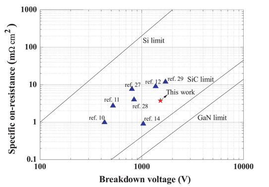
Figure 2: Summarized breakdown voltage and specific on-resistance for AlGaN/GaN HEMTs and MOS-HEMTs with various gate insulator materials.
Funding for the work came from a ‘Power Generation and Electricity Delivery’ grant of the Korea Institute of Energy Technology Evaluation and Planning (KETEP) government organization.
HfO2 gate insulator AlGaN AlGaN MOSHEMT
http://dx.doi.org/10.1088/0268-1242/28/2/025001
The author Mike Cooke is a freelance technology journalist who has worked in the semiconductor and advanced technology sectors since 1997.
