


- News
3 July 2013
Straining barriers towards low-noise high-breakdown pHEMTs
The UK’s University of Manchester has used band engineering on indium phosphide (InP) to create indium gallium arsenide (InGaAs) pseudomorphic high-electron-mobility transistors (pHEMTs) with reduced gate current leakage and high breakdown voltage [F Packeer, et al, J. Phys. D: Appl. Phys., vol46, p264002, 2013].
“The outstanding achievements of the new design approach are 99% less gate current leakage and a 73% increase in breakdown voltage, compared with the conventional design,” the researchers write. They hope that their work will lead to “implementation of outstanding low-noise devices”.
The researchers produced two epitaxial pHEMT structures (Figure 1) – one ‘conventional’ (XMBE171) and the other ‘advanced’ (XMBE210). The structures were grown using molecular beam epitaxy (MBE) on a Riber V100 machine.
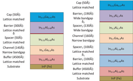
Figure 1: Epitaxial designs for XMBE171 conventional (left) and XMBE210 advanced pHEMTs.
The conventional structure consists of lattice-matched layers to the InP substrate, excluding the channel. In the advanced structure, the top barrier and spacer layers are strained in addition to the channel. Also, the advanced structure has two silicon delta-doped regions above and below the channel in place of the one region for the conventional setup.
The strain in the pseudomorphic indium gallium arsenide (In0.7Ga0.3As) channel is highly compressive compared with the lattice matched In0.53Ga0.47As. The advanced indium aluminium arsenide (In0.3Al0.7As) spacer and barrier layers are tensile strained compared with the lattice-matched In0.52Al0.48As.
Transistor fabrication was performed simultaneously on the two samples to avoid inconsistent devices from being compared in testing. Mesa isolation was achieved with a wet etch down to the InAlAs buffer. The main etch was with a non-selective orthophosphoric acid (H3PO4:H2O:H2O2) solution, followed by a sidewall etch with succinic acid solution to provide better isolation between the gate metal and channel during metallization.
The ohmic source-drain contacts consisted of evaporated gold-germanium and gold, alloyed at 280°C. The gate recess was achieved using a succinic acid solution selective etch through the cap layer. The gate consisted of evaporated titanium and gold. Bond pads were also evaporated, finishing the devices for probe testing.
Hall measurements gave 3.16x10¹²/cm2 carrier concentration and 10,653cm2/V-s mobility for the conventional pHEMT structure. The respective figures for the advanced structure were 2.70x10¹²/cm2 and 11,008 cm2/V-s. The reduced carrier concentration for the advanced structure is attributed to the thicker spacer (130Å) compared with the conventional pHEMT (50Å).
The effect of having a wider-bandgap InAlAs barrier layer in the advanced structure was expected to result in a larger Schottky barrier with the gate metal, reducing gate leakage. Such leakage occurs through thermionic tunneling in the off-state and through barrier crossing and impact ionization in the on-state. These effects are reduced by the higher Schottky barrier and thicker spacer in the advanced structure.
The double delta-doping is designed to improve confinement of the two-dimensional electron gas (2DEG) in the InGaAs quantum well. This, combined with the wide-bandgap InAlAs, should increase the Schottky breakdown voltage.
The reduced leakage current enabled the researchers to make advanced transistors with a gate width of 800μm (4x200μm). The conventional devices were constrained to widths of 200μm. The gate length was 1μm.
The lower carrier density in the 2DEG of the advanced pHEMT was reflected in the maximum drain current density (230mA/mm) and peak extrinsic transconductance (300mS/mm) being less than those of the conventional device (370mA/mm and 470mS/mm, respectively).
The advantages of the advanced structure begin to be shown by much reduced gate leakage currents: -9μA/mm in the -8V gate off-state, compared with -1000μA/mm at -5V for the conventional device. The advanced pHEMT leakage is more than “two orders of magnitude better, and therefore should provide excellent noise performance,” the researchers comment.
The off-state breakdown of 1mA/mm gate current is extrapolated to occur at -15V in the advanced device. The conventional device, by contrast, breaks the gate current limit in the -2V to -4V range. A high breakdown voltage is “excellent for designing low-noise amplifier receivers with minimal protection circuitry,” the researchers comment.
In the on-state range of -3V gate, the advanced device has a gate leakage of -0.2μA/mm, independent of drain bias up to 1V. The conventional device has a current in the range between -6mA/mm and -8mA/mm at the same gate potential, depending on drain bias. Beyond 1V drain, the gate leakage of the advanced device increases, but remains less than -16μA/mm range up to 2V bias. The comparable figure in the conventional device is -3.3mA/mm.
The researchers see this factor as potentially leading to low-noise and high-power applications.
The frequency performance of the devices was measured between 40MHz and 40GHz. The cut-off frequencies (fT) of the two devices were found to be the same at 21GHz.
“Therefore, the virtually identical fT of the advanced device to that of conventional structures demonstrates that the advanced pHEMT epitaxial design, with its high-tensile-strained supply layer, has had no detrimental effect on the device performance,” the researchers write.
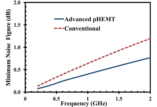 Figure 2: Comparison of minimum noise using Fukui’s analysis of conventional XMBE171 and advanced XMBE210 pHEMTs, up to 2GHz.
The advanced device showed ‘substantially’ improved Fukui minimum noise figure performance (Figure 2). A 1μm gate-length pHEMT would have expected low-noise applications for the range 300MHz-2GHz. The better noise performance is attributed to reduced current leakage. Further boosts come from the larger gate area due to reduced terminal resistance in the advanced pHEMT.
The researchers say that they are working on submicron gate lengths, presumably to increase frequency performance.
InGaAs pHEMTs InP substrates MBE
http://iopscience.iop.org/0022-3727/46/26/264002
The author Mike Cooke is a freelance technology journalist who has worked in the semiconductor and advanced technology sectors since 1997.
