


- News
13 June 2013
Longer-wavelength-lasing metamorphic InAs quantum wells on InP diodes
Chinese Academy of Sciences’ Shanghai Institute of Microsystem and Information Technology has extended the longest wavelength of indium phosphide-based antimony-free interband laser diodes to 2.7μm [Y. Y. Cao et al, Appl. Phys. Lett., vol102, p201111, 2013].
Laser light of such wavelengths has applications in molecular spectroscopy, gas analysis and medical inspection. The attractions of InP-based antimony-free structures include lower substrate costs, more mature processing technology, and better thermal conductivity, compared with the alternative of growing laser material on gallium antimonide (GaSb) substrates.
The epitaxial material (Table 1) was grown on (100) indium phosphide (InP) using a VG Semicon V80H gas-source molecular beam epitaxy (GSMBE) system. The InxAl1-xAs graded buffer was achieved by increasing the indium and lowering the aluminium temperatures to give x of 0.52 at the buffer layer and 0.84 at the beginning of the separate confinement heterostructure (SCH) laser material. The purpose of the grading is to provide ‘metamorphic’ strain compensation of the mismatch of the laser heterostructure and underlying InP substrate.
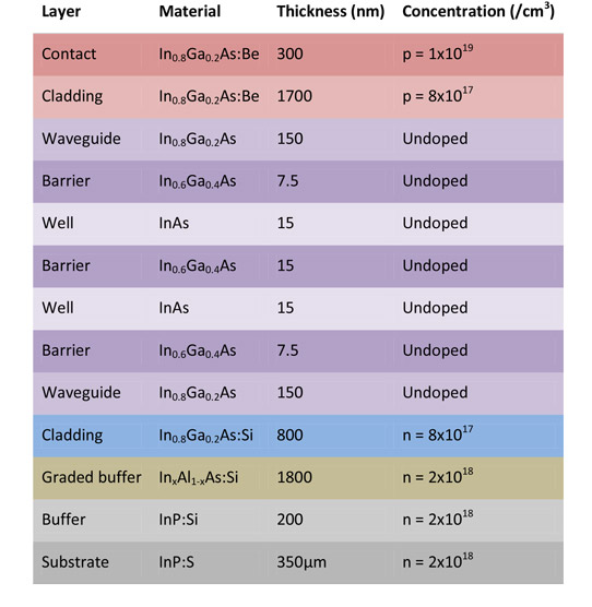
Table 1: Layer parameters of laser structure.
Ridge waveguide lasers were produced with a ridge width of 6μm. Isolation was achieved through plasma-enhanced chemical vapor deposition (PECVD) of 300nm of silicon nitride. A 4μm-wide hole opened in the silicon nitride on top of the ridge was filled with titanium/platinum/gold as a top metal contact. The devices were then thinned to 100-120μm and a back metal contact of germanium/gold/nickel/gold was applied. The devices were cleaved into 0.8μm-long bars, soldered on copper heat sinks and wire bonded. The facets were not coated.
Running in continuous wave (CW) operation at 1.2x the threshold current, the dominant lasing peak wavelength was 2.697μm at 77K and 2.71μm at 110K. The red-shift of 0.61nm/K on average was attributed to narrowing of the bandgap as the temperature increased.
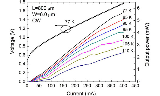
Figure 1: Current versus output power and voltage characteristics of laser under CW operation.
The threshold current was 7mA (145A/cm2 density) at 77K, and at 400mA injection current the output power was 5.7mW (Figure 1). The output power at 400mA decreased to 2.4mW at 110K. The relatively low characteristic temperature (T0) of 20.1K was possibly due to the narrower bandgap in the waveguide layers compared with the quantum well barriers, leading to unfavorable electron/hole confinement. The researchers believe that an optimized waveguide material could improve the electron/hole confinement, leading to better laser performance.
The threshold current density at 77K is lower than other values in the literature such as 290A/cm2 for a 2.45μm InP-based device at the same temperature, produced by a consortium of US-based researchers.
Laser diodes InAs quantum wells InP diodes GaSb substrates PECVD
http://link.aip.org/link/doi/10.1063/1.4807671
The author Mike Cooke is a freelance technology journalist who has worked in the semiconductor and advanced technology sectors since 1997.
