


- News
28 June 2013
China’s first diamond MESFET with gigahertz frequency performance
China-based researchers have reported that country’s first diamond metal-semiconductor field-effect transistors (MESFETs) with RF characteristics [Feng ZhiHong et al, Science China Technological Sciences, vol56, p957, 2013]. The team was based at four sites: Hebei Semiconductor Research Institute, Hebei University of Technology, University of Science and Technology Beijing, and Hebei Institute of Laser.
Diamond is of interest for high-power, high-frequency and high-temperature electronics due to its high breakdown field (~10MV/cm, which is 3.3x that of silicon carbide and 4x that of gallium nitride), its high thermal conductivity (~22W/cm-K, 4x SiC, 13x GaN), and its low dielectric constant (~5.7). Unfortunately, large-scale diamond manufacture is not available as yet.
The researchers used a 15mm x 15mm x 0.3mm free-standing polycrystalline film grown by arc melting. The polycrystalline grains were larger than 100μm – of the order of the size of the fabricated transistors. A p-type surface channel was created using a hydrogen plasma treatment. The treated samples had a surface channel carrier density of 1012/cm2 and mobility 20cm2/V-s.
Devices were fabricated using gold masks that were patterned using lithography. Gold masking was needed to avoid damage to the hydrogen termination of the diamond surface from oxygen plasma used to remove resist layers (Figure 1). Unannealed gold also makes a good ohmic contact with the hydrogenated diamond surface with a specific resistivity of 10-5Ω-cm2.
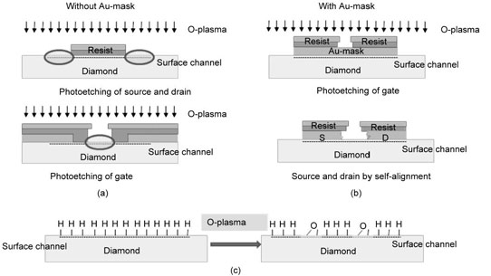
Figure 1: (a) The lithography process with (a) and without (b) Au-mask. Damaged areas are indicated by circles; (c) O-plasma on hydrogen-terminated diamond surfaces.
The devices were isolated using an oxygen plasma mesa etch. A selective etch of the gold with potassium iodide created the source and drain electrode regions. The 2μm Schottky gate was made from aluminium. The gate width was 2x100μm.
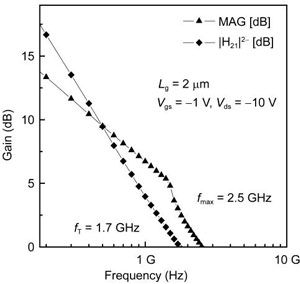 Figure 2: RF gain plot of the polycrystalline diamond MESFET at –1V gate and –10V drain.
The maximum drain current density was increased to 204mA/mm when using gold masking, compared with 22mA/mm without gold masking. The maximum drain current density of 204mA/mm was achieved with a negatively biased gate of –6V. The maximum transconductance was 20mS/mm at –1.5V gate, and the off-state breakdown voltage was –47V.
The extrinsic cut-off and maximum oscillation frequencies were 1.7GHz and 2.5GHz, respectively (Figure 2). The researchers believe that these values can be improved with shorter gate lengths. Outside of China, diamond MESFETs with frequency performance values of tens of gigahertz have been fabricated.
The frequency response was lower than expected. This could be attributed to the effects of the grain boundaries and problems with crystal quality inside the grains.
http://link.springer.com/article/10.1007/s11431-013-5163-z
The author Mike Cooke is a freelance technology journalist who has worked in the semiconductor and advanced technology sectors since 1997.
