


- News
11 June 2013
Overgrowth and surface plasmons for ultraviolet LEDs made on silicon wafers
Northwestern University’s Center for Quantum Devices (under the direction of professor Manijeh Razeghi) has developed a surface-plasmon (SP) enhancement technique for ultraviolet (UV) light-emitting diodes (LEDs) produced on silicon substrates [Chu-Young Cho et al, Appl. Phys. Lett., vol102, p211110, 2013]. The resulting devices achieved a peak output power of 1.2mW at wavelengths around 346nm.
The use of silicon as a substrate for nitride semiconductor structures has been of much interest in the past few years for high-power and high-frequency transistors. Silicon offers the prospect of lower costs, economies of scale from the availability of larger-diameter wafers, and so on. More recently, researchers have turned to the more difficult challenge of producing light-emitting devices using nitride semiconductors grown on silicon.
Northwestern has developed techniques to improve the crystal quality of the nitride semiconductor growth on silicon and in addition used aluminium (Al) metal structures to boost quantum efficiency with coupling to surface plasmons (collective oscillations of free electrons at metal-dielectric interfaces).
The epitaxial material was grown on (111) silicon using low-pressure metal-organic chemical vapor deposition (MOCVD). Lateral epitaxial overgrowth (LEO) was used to improve the quality of the initial aluminium nitride (AlN) layer. It is particularly difficult to grow AlN on silicon due to the large ~19% lattice mismatch between their crystal structures.
The LEO method consisted of first growing a thin 100nm layer of AlN, etching a 2μm-wide stripe pattern with a period of 4μm to expose regions of silicon, and the re-growth of a thick 8μm layer of AlN with reduced dislocations and cracks. The growth steps used a high temperature (1300°C) and atomic layer epitaxy, achieved using pulses of the different precursors.
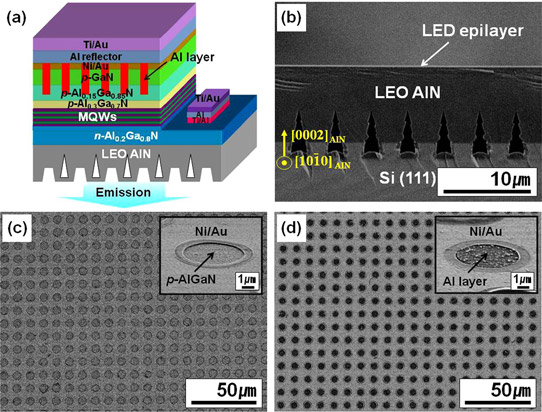
Figure 1: (a) Schematic diagram of the SP-enhanced AlGaN-based UV LED structure with embedded Al layer. (b) Cross-sectional SEM image of LED structure grown on Si (111) substrate. Plan-view SEM images of circular-shaped holes in p-contact layer (c) before and (d) after deposition of the Al layer.
After the AlN growth the material was found to have air-voids (Figure 1b) where the material had grown laterally and then coalesced to form the AlN template for the subsequent layers. “These voids decouple the top AlGaN layers from the silicon substrate and help avoid the formation of cracks,” the researchers write.
Further epitaxial layers consisted of 600nm of n-type aluminium gallium nitride (n-Al0.2Ga0.8N), a multiple quantum well (MQW) active region, 10nm of p-Al0.3Ga0.7N for electron blocking, 50nm p-Al0.15Ga0.85N cladding, and a 50nm p-GaN contact. The MQW consisted of three 3nm Al0.1Ga0.9N wells separated by 7nm Al0.15Ga0.85N barriers. The MQW was grown at a reduced temperature of 1150°C.
LED fabrication consisted of electron cyclotron resonance reactive ion etch (ECR-RIE) of 300μm x 300μm square mesas, the application of a titanium/aluminium ohmic n-contact, and the deposition of a nickel/gold ohmic p-contact. Surface-plasmon enhancement was achieved by drilling 5μm holes 90nm deep into the p-type GaN/AlGaN layers with ECR-RIE. These holes (with 10μm period) were filled with Al metal.
The researchers used Al surface plasmons since their energy is in resonance with the ~340nm UV light of the AlGaN LED structure. To couple surface plasmons with the radiation in the MQW, the Al metal needs to be close by, of the order of tens of nanometers. The penetration depth of the SP fringing field was estimated at ~50nm. In the Northwestern LEDs, the pillars were 20nm away from the MQW.
The devices were completed with an Al reflector, and titanium/gold layers were added to both n- and p-contacts. The chips were flipped onto AlN submounts and the silicon substrate was chemically removed.
As is usual, the structures were first tested for photoluminescence (PL), with the SP-MQW devices showing an enhancement of 2.4x integrated intensity at room temperature. This is more than would be expected from just having an Al mirror (< 2x).
The researchers comment: “This improvement of the PL intensity is believed to be due to an increase in the spontaneous emission rate and improved internal quantum efficiency of MQWs by SP-coupling.”
Normalizing with respect to PL measurements at 10K, where the internal quantum efficiency (IQE) is estimated to be 100%, the IQE without Al structures was 3.7%, increasing to 10.1% with SP-MQW structures. It is thought that the coupling of SPs with the excitons (electron-hole pairs) in the MQW region increases the spontaneous recombination rate and hence improves IQE.
Tests with structures where the distance between the MQW and Al SPs is increased by inserting a silicon dioxide spacer supports the concept of SP-MQW coupling.
Devices with and without Al SP structures had very similar current-voltage behavior. This is encouraging, since etch processes can degrade electrical performance.
The improved performance of Al SP structures carried over to the full LEDs (Figure 2). A maximum output power of 1.2mW was achieved with an injection of 700mA current, a 45% improvement over the device without Al SP structures. Pulsed operation was used to avoid performance degradation from self-heating effects.

Figure 2: (a) Room-temperature EL spectra of UV LEDs with and without Al layer. Inset: inclined plan-view SEM images of SP-enhanced UV LED bonded to AlN submount after removal of Si substrate. (b) Optical output power of UV LEDs with and without Al layer versus injection current.
The researchers explain the smaller improvement for electroluminescence (EL), as compared with PL, as being due to the PL including enhancements of both energy absorption and emission.
UV-LEDs Silicon wafers AlN MOCVD LEO
http://link.aip.org/link/doi/10.1063/1.4809521
The author Mike Cooke is a freelance technology journalist who has worked in the semiconductor and advanced technology sectors since 1997.
