

- News
5 March 2013
AKHAN licenses Argonne’s low-temperature diamond deposition technology
AKHAN Technologies Inc of Hoffman Estates, IL, USA has been granted exclusive diamond semiconductor application licensing rights to low-temperature diamond deposition technology developed by the Center for Nanoscale Materials (CNM) at the US Department of Energy’s Argonne National Laboratory.
AKHAN was founded by CEO Adam Khan in 2007 to commercialize Diamond Lattice Technology, with the main aim being to introduce diamond device technology for the commercial realization of diamond-based electron devices for both the digital and discrete semiconductor markets.
The Argonne-developed technology allows the deposition of low-defect nanocrystalline diamond (NCD) thin films on a variety of wafer substrate materials at temperatures as low as 400°C, which is advantageous for integration with processed semiconductor electronic materials. Argonne’s low-temperature diamond technology can be combined with AKHAN’s Miraj Diamond process to provide diamond semiconductor thin-film technology. AKHAN debuted its Miraj Diamond platform in November 2011 in a series of patent filings and technical journal submissions.
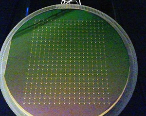 Picture:
A wafer of nanocrystalline diamond. (Photo courtesy of Ani Sumant.)
Picture:
A wafer of nanocrystalline diamond. (Photo courtesy of Ani Sumant.)
AKHAN says that, with the acquisition of Argonne’s low-temperature diamond technology, it plans to fabricate thin-film n-type NCD devices on 4” fused silica (glass) wafers at a CMOS-compatible thermal budget. “The vertically integrated development capability now afforded through the combination of IP will allow for both next-generation-performance devices and lower per-unit costs more conducive to present global industry demands,” comments Khan.
“This licensing agreement gives us the impact of a one-two punch, in which we combine AKHAN’s novel process to achieve efficient n-type doping in diamond with Argonne’s low-temperature diamond deposition technology,” says Argonne nanoscientist Anirudha Sumant, co-inventor of the Argonne IP. “This will break barriers that restricted the use of diamond thin films in the semiconductor industry limited to only p-type doping,” he adds. “The AKHAN process will allow us to fabricate efficient p-n junction devices based on diamond, which was not possible before, and Argonne’s technology will allow integration with the existing CMOS platform.”
“It is always wonderful to see when basic materials research leads to promising new technology developments,” comments Andreas Roelofs, Argonne's CNM deputy division director and industrial relations liaison. “Having a company license your technology is the best proof of showing that you are working on relevant questions.”
AKHAN and Argonne are planning to develop this further through a Cooperative Research and Development Agreement (CRADA) initiative. “We are looking forward to the further developments in diamond technology and hope to continue our successful collaboration with AKHAN in the future,” adds Roelofs.
As part of a recent collaborative project, AKHAN and Argonne researchers were able to demonstrate working diamond devices with improved performance using the Miraj Diamond process based on conventional high-temperature nanocrystalline diamond. AKHAN also announced the availability of published characterization data of its Miraj Diamond technology in the Materials Research Society (MRS) Online Proceedings Library (see link below). In the paper ‘On Enabling Nanocrystalline Diamond For Device Use: Novel Ion Beam Methodology and The Realization Of Shallow N-Type Diamond’, AKHAN and Argonne researchers confirm what is claimed to be breakthrough morphological, phase, and electrical characterization data for both n-type NCD wafer material and NCD PIN diode devices. The full paper is available through Cambridge Journals Online.
http://journals.cambridge.org/action/login
