

- News
29 March 2013
Thermal anneal for improving adhesion of gold-doped graphene to nitride LEDs
Researchers in South Korea have developed a new gold-doping process for graphene transparent conducting layers (TCLs) that improves its adhesion and electrical contact with near-ultraviolet light-emitting diodes (NUV-LEDs) [Chu-Young Cho et al, J. Appl. Phys., vol113, 113102, p2013].
TCLs are used to improve current spreading and efficiency of NUV-LEDs. A common TCL material for visible light is indium tin oxide (ITO), which unfortunately becomes opaque in the UV range. The optical transmittance of graphene extends further into the UV than ITO.
The team consisted of researchers from Gwangju Institute of Science and Technology, Seoul National University, and Samsung Electronics Co Ltd. Some of the same researchers were involved in research at Gwangju Institute of Science and Technology, Korea Basic Science Institute Jeonju Center, and Seoul National University that previously developed a solution-based gold-doping process to improve the conductivity of graphene TCLs [Boosting transparent conduction in graphene with gold nanoparticles]. This latter technique was found to suffer from poor adhesion to the underlying gallium nitride (GaN) semiconductor p-contact layer.
The new technique began by producing multi-layer graphene (MLG) through chemical vapor deposition (CVD) on a 300nm layer of nickel on a silicon dioxide/silicon substrate. The carbon source was methane in hydrogen and argon. The growth temperature was 900°C. After rapid cooling to avoid excessive carbon precipitation, the multi-layer graphene was released by etching in iron chloride aqueous solution.
The floating graphene films were directly transferred to NUV LED structures produced by metal-organic chemical vapor deposition (MOCVD) – see Figure 1. The emission wavelength of the 5-period indium gallium nitride (InGaN) multi-quantum well (MQW) structure with GaN barriers was 415nm. The LED structure was etched by inductively coupled plasma to expose an n-contact area.
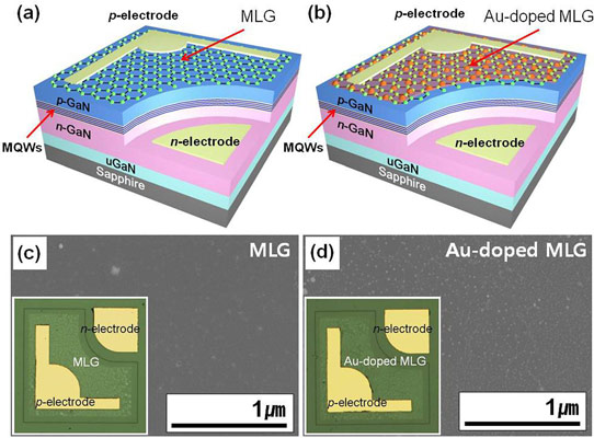
Figure 1: Schematic diagrams of NUV-LEDs with (a) MLG and (b) Au-doped MLG TCLs. (c) and (d) SEM images of MLG and Au-doped MLG. Inset: optical microscopy images of NUV-LEDs with MLG and Au-doped MLG TCLs.
After the MLG transfer, the p-electrode and n-electrode regions were selectively cleared of MLG material through photolithography and reactive-ion etching.
The gold-doping of the MLG was achieved by depositing 0.2nm of the metal onto the surface using electron-beam evaporation, followed by annealing at 700°C for 5 minutes in nitrogen. It was found that this method improved the adhesion between the MLG and GaN.
Previously, the researchers had found that MLG only weakly adhered to GaN, resulting in easy detachment of the MLG in lift-off processes and in a poor electrical contact between the materials that degraded LED performance.
The researchers think that the adhesion is improved by the formation of gold (Au) nanoparticles and diffusion of gold into the p-GaN material. They also believe that the thermal anneal step could remove oxidized p-GaN and residual chemicals, further improving MLG/LED adhesion.
The n- and p-pad electrode metals were both chromium/gold.
Atomic force microscope (AFM) study of the surface showed that thermal annealing transforms the gold layer into ~50nm-diameter and ~8nm-high nanoparticles. Optical transmittance study of the layer gives a value of 88% for 415nm light, about the same as for bare MLG. This compares with 80% for 200nm indium tin oxide. MLG with unannealed gold has somewhat depressed transmittance. Further into the UV, annealed gold-nanoparticle MLG has improved transmittance compared with bare MLG.
At 20mA injection current, the forward voltage of the LED with annealed gold-doped MLG TCL is 6.8V, reduced from 7.8V for the bare-MLG device. This indicates reduced resistance for the gold-doped layer. The sheet resistance of the annealed gold MLG was 18Ω/square, compared with 1000Ω/square for the previously developed MLG treated with gold chloride solution.
The researchers comment that “the improved I-V characteristics of the NUV-LEDs with an Au-doped MLG layer can be attributed to the reduced sheet resistance of the Au-doped MLG films and the decreased contact resistance between Au-doped MLG and p-GaN layer.”
Electroluminescence was also much increased with annealed gold-doped MLG TCL (Figure 2). More effective current injection and spreading also lead to more uniform and stronger emissions.
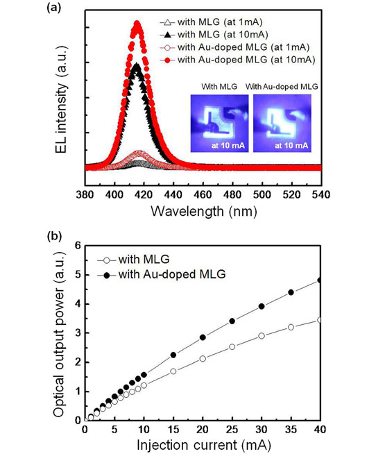
Figure 2: (a) Room-temperature electroluminescence spectra of NUV-LEDs with MLG and Au-doped MLG TCLs, measured at 1mA and 10mA. Inset: photographs of NUV-LEDs with MLG and Au-doped MLG TCLs at 10mA. (b) Optical output power of NUV-LEDs with MLG and Au-doped MLG TCLs.
Spectral analysis indicates a slight blue shift to 413nm in moving from 1mA to 10mA current. This is attributed to screening of “polarization-induced electric field by carriers and a band-filling effect of localized energy states formed by potential fluctuation in MQWs”.
At 20mA, the optical power output of the gold-doped MLG LED is increased by 34% over a device with bare MLG TCL. “This improvement of the optical output power of NUV-LEDs is attributed to the increased current injection efficiency, current spreading, and transmittance of Au-doped MLG TCL,” the researchers write.
Boosting transparent conduction in graphene with gold nanoparticles
http://link.aip.org/link/doi/10.1063/1.4795502
The author Mike Cooke is a freelance technology journalist who has worked in the semiconductor and advanced technology sectors since 1997.
