

- News
21 March 2013
New orientation for gallium nitride on silicon transistors
The first millimeter-wave power demonstration of aluminium gallium nitride/gallium nitride (AlGaN/GaN) high-electron-mobility transistors (GaN) grown on a (110) silicon substrate has been claimed by a French team of researchers [A. Soltani et al, IEEE Electron Device Letters, published online 7 March 2013]. The team consists of workers from Institut d’Electronique, de Microélectronique et de Nanotechnologie (IEMN) and Centre de Recherche sur l'Hétéro-Epitaxie et ses Applications (CRHEA).
GaN-based transistors are promising for future high-frequency/high-power devices such as RF power amplifiers for wireless network base-stations. Also, the material is being developed for power switching that needs to operate at high voltages and temperatures. Traditional growth substrates for GaN such as sapphire and silicon carbide are expensive and there has been a combined industry-research push to develop high-performance devices on lower-cost silicon substrates. In addition, silicon is available in much larger-diameter formats (up to 300mm) that offer potential economies of scale.
Most reports of silicon substrate nitride semiconductor transistors up to now have used the (111) orientation because it offers a hexagonal surface crystal structure onto which it would appear to be most natural for the hexagonal nitride semiconductor wurtzite structure to grow. Mainstream silicon semiconductor production prefers the (001) orientation, but GaN growth is more difficult because the surface has square symmetry. One particular problem with (001) growth is cracking of GaN material thicker than 1μm.
Recently, researchers have suggested using (110) silicon since it has a quasi-lattice that is matched with AlN. Aluminium nitride is often used for nucleation layers before the growth of thick GaN buffers on silicon. Another potential advantage is that (110) silicon has much better electron transport properties than (111) silicon, raising the prospect of silicon/GaN electronics co-integration.
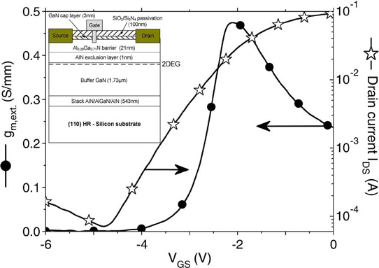
Figure 1: Transfer (drain current IDS) and extrinsic transconductance (gm,ext) characteristics versus gate potential VGS at 10V drain bias for IEMN/CRHEA HEMT. Inset shows cross section of fabricated AlGaN/GaN HEMT.
The epitaxial material for the IEMN/CRHEA transistor was grown using molecular beam epitaxy (MBE) on 2-inch high-resistivity (HR, more than 5kΩ-cm) silicon with (110) surface orientation. The initiation layer was 43nm aluminium nitride (AlN). This was followed up with a stress-mitigating stack of 250nm aluminium gallium nitride (Al0.15Ga0.85N) and 250nm AlN. This was followed by buffer, exclusion/spacer, and barrier layers (Figure 1). The aim of the exclusion layer was to reduce alloy scattering and to improve confinement of the two-dimensional electron gas (2DEG) channel.
Simulation suggested that the stress-mitigation stack could also provide a back-barrier equivalent to that provided by a 1μm-thick Al0.15Ga0.85N layer 10nm from the active area.
Scanning electron microscopy and atomic force microscopy inspection of the epitaxial material did not find any surface cracking. The threading dislocation density was estimated at 3.7x10⁹/cm2, similar to the level found with GaN on (111) silicon.
The transistors that were produced had 60nm-long T-gates with 10nm recess depth. The gate width was 2x30μm. The source-drain distance was 2μm and the source-gate distance 0.15μm. The ohmic source-drain contacts were recessed to 18nm to reduce contact resistance.
The ohmic contact recess was achieved using argon ion milling. The contact electrodes consisted of titanium/aluminium/nickel/gold annealed at 870°C for 30 seconds in nitrogen.
Electrical isolation was achieved using helium ion implantation. Surface passivation consisted of nitrous oxide (N2O) pretreatment, followed by silicon nitride/silicon dioxide bilayer plasma-enhanced chemical vapor deposition.
Formation of the T-gate consisted of patterning, reactive-ion etch, recessing in the barrier using argon ion milling and 4nm depth digital etch, and metallization with nickel/platinum/titanium/molybdenum/gold. Thick titanium/gold metal interconnect lines were added using lift-off techniques.
The completed device was finally annealed at 400°C for 20 minutes in nitrogen with the aim of electrically stabilizing the rectifying contact of the Schottky gate. The measured reverse leakage current of the gate was -30μA/mm at -10V.
Hall measurements of the epitaxial material gave carrier mobility of 2045cm2/V-s with density 1.21x10¹³/cm2, and sheet resistance 245Ω/square. Capacitance-voltage measurements under reverse bias found that the 2DEG was located 24nm below the surface.
The maximum DC drain current of 1.55A/mm was achieved at 10V drain and 0V gate potentials. The peak extrinsic transconductance of 476mS/mm was obtained at -2.2V gate potential. Pinch-off occurred with the gate at -3.9V. Three-terminal off state breakdown (1mA/mm drain current) occurred at 24V drain-gate bias.
The researchers estimate the peak intrinsic transconductance at 566mS/mm. “This high transconductance value can be explained by the low source access resistance (evaluated to 5.6Ω for LGS = 150nm),” the researchers comment.
The cut-off (fT) and maximum oscillation (fmax) frequencies at -2.2V gate and 4V drain were 81GHz and 106GHz, respectively.
Pulsed measurements (400ns, 0.4% duty cycle) were carried out to determine trapping and thermal effects. Under gate pulsing from -6V to 0V and drain pulsing from 0V, the maximum drain current was 1.67A/mm, a drop of 6.2% indicating some gate lag effects. Drain lag effects were investigated by pulsing from the quiescent point of 15V drain and -6V gate. In this case, the current dropped 20.9%.
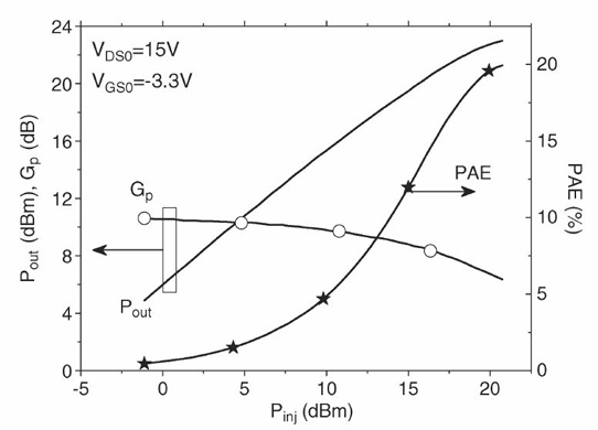
Figure 2: CW power performance of IEMN/CRHEA HEMT at 40GHz.
The researchers considered the lag effects small enough for reproducible and high microwave power performance. A continuous-wave active load-pull measurement at 40GHz was performed in conjunction with a large-signal network analyzer working up to 50GHz. There was no external cooling applied. The device achieved a saturated output power of 2.3dBm (3.3W/mm) with associated power gain of 10.6dB and power-added efficiency (PAE) of 20.1%.
Similar 40GHz measurements on devices produced on (111) silicon have been reported that gave 2W/mm output power with an AlGaN barrier and 2.5W/mm with an AlN barrier. A device produced on (001) silicon has achieved 2.9W/mm at the lower frequency of 10GHz.
HEMTs GaN Silicon substrates MBE
http://ieeexplore.ieee.org/xpl/articleDetails.jsp?tp=&arnumber=6471741
The author Mike Cooke is a freelance technology journalist who has worked in the semiconductor and advanced technology sectors since 1997.
