

- News
8 March 2013
Laser-processed sapphire allows increased thickness of HVPE GaN
Researchers in Japan and Switzerland have used a laser treatment of sapphire substrates to increase the thickness of gallium nitride (GaN) layers grown by hydride vapor phase epitaxy (HVPE) to around 200μm [Hideo Aida et al, Appl. Phys. Express, vol6, p035502, 2013]. The researchers were based at Namiki Precision Jewel Co Ltd, École Polytechnique Fédérale de Lausanne (EPFL), Namiki Precision of Europe SA, and Ritsumeikan University.
HVPE is an attractive GaN growth technology since it is much more rapid than metal-organic chemical vapor deposition (MOCVD) or molecular beam epitaxy (MBE). Growth speeds for HVPE can reach hundreds of microns per hour. However, the approach is presently limited by differences in lattice constants and thermal expansion between sapphire and GaN. In particular, the sapphire substrate tends to crack on cooling with thicker GaN layers. On the other hand, thicker layers are desired for reducing the effects of threading dislocations (TDs) and for developing free-standing GaN substrates.
The researchers used 1045nm femtosecond laser light to control stress in the c-plane sapphire substrates (Figure 1). The laser light was focused within the sapphire material to create amorphous layers without damaging the crystalline surface used for epitaxy. The effect of the amorphous regions is to create strain due to volume expansion. Various laser treatments were performed: A, with the laser focused in the upper half of the substrate thickness, giving a 70μm bowing effect; B, with the laser focused in the middle of the thickness, giving near-zero bowing; and C, with two amorphous regions from focusing the laser in the upper and lower halves, again giving near-zero bowing.
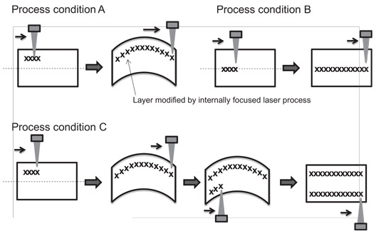
Figure 1: Schematic of laser processing within the substrate and the related substrate bow changes.
The HVPE growth began with nitridation and ex-situ surface preparation. The substrate was then returned to the HVPE reactor for thick GaN growth. The researchers liken their procedure to the two-step process (low-temperature nucleation/high-temperature growth) for GaN metal-organic chemical vapor deposition.
On an unprocessed substrate, the critical thickness was 15‑20μm before the GaN template cracked. For layers greater than 80μm, the substrate shattered (Figure 2). Laser-treated substrates allowed much thicker layers to be grown (Table 1).
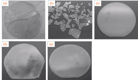
Figure 2: Photographs of the GaN layers on sapphire substrates: (a) 50μm GaN on plain sapphire (S-substrate), (b) 80μm GaN on S-substrate, (c) 80μm GaN on A-substrate, (d) 200μm GaN on the B-substrate (slight cracks seen at edge giving near-hexagonal shape), and (d) 200μm GaN on C-substrate (no cracking).
Beyond the critical thickness, the cracks seem to be generated during the cooling process due to differences in coefficient of thermal expansion between sapphire and GaN. Another effect of the laser treatment seems to be that the sapphire is able withstand greater amounts of bowing before cracking. The researchers speculate that the laser process may improve the flexibility of the sapphire substrate under bending stress.
| Substrate | Critical thickness | Extracted critical bow |
| S | 15–20μm | 116–138μm |
| A | 80–90μm | 423–466μm |
| B | 190–210μm | 623–669μm |
| C | 220–250μm | 547–613μm |
Table 1: Critical GaN thickness and extracted critical bow for crack generation of sapphire substrates.
The quality of the GaN material was analyzed using cathodoluminescence (CL) and atomic force microscopy (AFM). The threading dislocation density of thin layers grown on plain sapphire was estimated to be 2x10⁸/cm2. This was reduced to 1x10⁷/cm2 for a 200μm GaN layer grown on a laser-processed substrate. It is thought that the reduction in TDs is due to the mutual annihilation of dislocations.
HVPE GaN Laser Sapphire substrates
http://apex.jsap.jp/link?APEX/6/035502
The author Mike Cooke is a freelance technology journalist who has worked in the semiconductor and advanced technology sectors since 1997.
