

- News
6 May 2013
Strain engineering improves light output from green LEDs
Researchers in China have used strain engineering to improve the light output power of 530nm green light-emitting diodes (LEDs) by 28.9% at 150mA current injection [Hongjian Li et al, Appl. Phys. Express, vol6, p052102, 2013]. The research was carried out by Chinese Academy of Sciences’ Institute of Semiconductors, Beijing, and University of Hong Kong.
Green-emitting nitride semiconductor LED structures tend to suffer from low light output due to the difficulty in producing the high-indium-content indium gallium nitride (InGaN) needed for longer-wavelength light emission. Apart from the material quality challenge, strain induced by the lattice mismatch with pure GaN leads to large piezoelectric effects, giving electric fields that tend to pull electrons and holes apart, reducing rates of recombination into photons (i.e. the quantum-confined Stark effect, or QCSE).
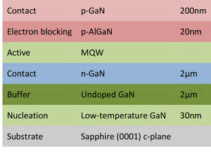 Figure 1. Schematic of epitaxial material for conventional and shallow quantum well (SQW) LEDs.
The Chinese team tackled the problem by inserting a layer of lower-indium-content InGaN before the high-In-content light-emitting layer. Simulations were carried out first, suggesting that such a layer could reduce the strain-dependent electric fields in the active light-emitting multiple quantum well (MQW) structure.
Epitaxial material with a low-In-content InGaN shallow quantum well (SQW) step was realized using metal-organic chemical vapor deposition (MOCVD) on c-plane (0001) sapphire (Figure 1). Conventional device structures were also produced. The conventional multi-quantum well (MQW) active region consisted of 12 periods of 3nm In0.3Ga0.7N wells between 12nm GaN barriers. The SQW structure consisted of 12 periods of a 2nm In0.1Ga0.9N shallow well and a 3nm In0.3Ga0.7N deeper well between 12nm GaN barriers. These materials were then fabricated into 256μm x 300μm mesa-structure LED chips.
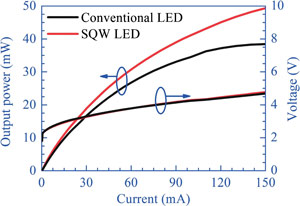 Figure 2. Light output power–current–voltage (L–I–V) characteristics of conventional LED and SQW LED.
A 325nm helium-cadmium laser was used to excite the photoluminescence spectra of the materials at low temperature (85K) and room temperature (298K). One effect of the SQW was to reduce the width of the spectral peak full-width at half maximum (FWHM) at 85K from 16.7nm for the conventional LED material to 13.1nm for the SQW material. The 298K measurement reduced the conventional FWHM of 20.1nm to 15.7nm.
The peak intensity was also higher with the SQW structure. These results are taken as indicating improved crystal quality for the SQW material. In particular, the narrow FWHM suggests “more uniform indium distribution and less carrier localization within the active region” due to lower stress in the active region.
The peak height for the SQW material at 298K was 55.1% that at 85K. The corresponding ratio for the conventional structure was 24.1%. The higher ratio for the SQW material indicates a higher rate of radiative recombination and higher internal quantum efficiency (IQE) due to a smaller QCSE.
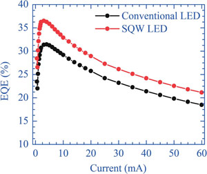 Figure 3. EQE versus current characteristics of conventional LED and SQW LED.
The electroluminescence was measured in an integrating sphere, giving light output power–current–voltage (L–I–V) results (Figure 2). The voltage performance is similar in the SQW and conventional devices. However, the light output at 150mA is 28.9% greater in the SQW LED (49.3mW) over the conventional device (38.4mW).
The researchers attribute the enhanced results for the SQW LED to improved overlap of the electron and hole wavefunctions in the device, leading to improved recombination into photons. The performance is not enhanced to the same extent as for photoluminescence because the biasing in electroluminescence increases the polarization fields.
The external quantum efficiency (EQE) is increased 10.2–13.3% over the conventional LED performance (Figure 3).
http://apex.jsap.jp/link?APEX/6/052102
The author Mike Cooke is a freelance technology journalist who has worked in the semiconductor and advanced technology sectors since 1997.
