


- News
15 November 2013
Thinning gallium nitride barriers for more efficient photovoltaic conversion
University of California Santa Barbara (UCSB) and Fuji Electric Corp of America have been developing indium gallium nitride (InGaN) solar cell structures in efforts to extend the conversion efficiency of multi-junction photovoltaic (PV) devices to shorter photon wavelengths [N. G. Young et al, Appl. Phys. Lett., vol103, p173903, 2013].
Existing three- and four-junction PV devices are limited to converting photons with energies less than 2eV (620nm, red-orange). According to theoretical analyses, a further semiconductor junction with an absorbing material having a bandgap around 2.6eV (480nm, blue) is needed to utilize higher-energy photons.
Indium gallium nitride is a material system capable of creating such bandgaps. However, InGaN with indium fractions above 20% is tricky to grow with sufficient thickness and quality to convert these high-energy photons. The material is generally grown on gallium nitride and can only be applied in thin nanometer-scale layers before the crystal quality degrades. Hence, InGaN for light emission is usually grown in a series of thin layers separated by GaN barriers, creating multiple quantum wells (MQWs). In light-emitting diodes the wells are often less than 5nm thick, while barriers are more than 10nm.
Unfortunately, the barriers impede carrier extraction and also create other electrical problems, so it is desired to reduce the barrier thickness as much as possible. UCSB reported last year a technique for growing InGaN MQWs with thinner GaN barriers, and have now applied the method to create PV structures with up to 50 wells.
The UCSB/Fuji researchers grew the InGaN multiple quantum wells for the solar cells (Figure 1) on co-loaded sapphire and bulk GaN substrates using metal-organic chemical vapor deposition (MOCVD). The sapphire substrate was half of a 50mm-diameter wafer that included a 2μm n-GaN template layer. The 5mm x 5mm bulk GaN was supplied by Furukawa Denshi Co Ltd from a hydride vapor phase epitaxy (HVPE) process.
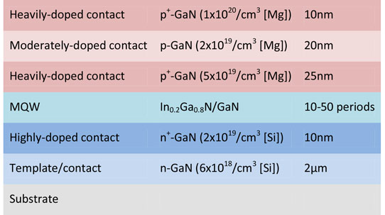
Figure 1: MQW structure of InGaN solar cells.
The bulk GaN had a threading dislocation density (TDD) of 3x10⁶/cm2, while the n-GaN template on the sapphire substrate had a TDD value at least two orders of magnitude greater.
The active region consisted of 10-to-50-period MQWs consisting of 2.3nm wells on sapphire and 3.0nm wells on bulk GaN. The researchers do not fully understand the different well thicknesses given the same process conditions. High-angle annular dark-field imaging with a scanning transmission electron microscope (HAADF-STEM) showed ‘severe’ well thickness fluctuations on sapphire substrates.
The GaN barrier layers were 4.0nm on both substrates. The thinness of the barriers was achieved by using a low temperature to deposit a 2nm GaN cap on the InGaN and then adding the remaining 2nm at high temperature in hydrogen “to improve surface adatom mobility and effectively fill in the V-defects”. (V-defects tend to nucleate on pre-existing threading dislocations, creating losses through recombination centers and current leakage.) This process had previously been developed and optimized at UCSB to achieve thinner barriers than previously achieved. HAADF-STEM analysis of the bulk GaN structure showed slight variation in barrier thickness.
The solar cells were fabricated by standard techniques: 1mm x 1mm mesa isolation plasma etch, evaporation of palladium/gold p- electrodes in a grid pattern, and deposition of aluminium/gold n-electrodes onto the n-GaN contact material at the base of the mesa.
The 50x MQW devices showed increased external quantum efficiency (EQE) and absorption over the thinner MQW devices. The spectral response extended down to 460nm. The peak EQE was 60% on bulk GaN. For the sapphire-based devices the improvements with more MQWs fell off significantly beyond the cell with 20x MQW.
Current-voltage measurements in dark and illuminated conditions gave open-circuit voltages up to 2.28V and fill factors up to 80% (Figure 2). The researchers consider the best device to be one with a 30x MQW active region grown on bulk GaN. For this cell the peak EQE was 51.2%, the open-circuit voltage 2.26V, the fill factor 70.4%, the short-circuit current density 2.10mA/cm2, and the maximum power density 3.33mW/cm2 (33.3W/m2). The conversion efficiency came out at 2.5% on the basis of the input integrated power density of 1336.1W/m2 under the AM0 standard. (AM0 represents the radiation intensity from the sun as seen in the vacuum of outer space, as needed for artificial satellite/space applications.)
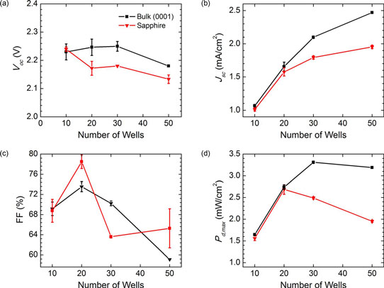
Figure 2: Dependence of (a) open-circuit voltage, (b) short-circuit current density, (c) fill factor, and (d) maximum power density on number of QWs for samples grown on co-loaded bulk (0001) GaN and sapphire substrates.
The bulk GaN substrate devices showed generally improved performance over the sapphire cells, except for the fill factor (maximum power as a fraction of the product of open-circuit voltage and short-circuit current). This is partly a result of reduced numbers of V-defects that tend to emanate from the threading dislocations and then propagate through the MQW region.
Above 20 wells, sapphire-based cells showed pits on the surface, indicating V-defects in atomic force microscopy (AFM) analysis. By contrast, the bulk GaN cells were smooth and pit-free up to 50 wells. However, beyond 30 wells the bulk GaN cells did show a decline in performance.
Some of the improved solar cell performance from material grown on bulk GaN can be attributed to the thicker wells compared with the material grown on sapphire. HAADF-STEM study also showed some defects arising in the quantum well structure itself rather than being propagated from the underlying material. The researchers suggest that this would lead to a drop off in performance for the thicker MQW structures on bulk GaN beyond 30 periods.
The 30-period MQW on bulk GaN solar cell is still some way off from the theoretically ideal performance for an InGaN structure (Table 1). The main deficit in performance is related to the short-circuit current. The researchers say the limiting factor for the current density is the thickness of InGaN that can be grown before the onset of structural instabilities due to mismatch stresses. Such stresses degrade the absorbing material quality and hence solar cell performance.
Table 1: Comparison of device parameters between values measured for the 30 QW InGaN/GaN solar cell on bulk (0001) GaN and values for an ideal InGaN-based solar cell with the same bandgap.
| Parameter | Measured | Theoretical | Percent of ideal |
| Short-circuit current | 2.10mA/cm2 | 6.23mA/cm2 | 33.7% |
| Open-circuit voltage | 2.26V | 2.343V | 96.5% |
| Fill factor | 70.4% | 89.5% | 78.7% |
| Maximum output power | 3.33mW/cm2 | 13.06mW/cm2 | 25.5 |
The research team comments: “One possible solution for preventing strain-related degradation is a strain-balanced InGaN/AlGaN MQW active region, though any solution will involve significant materials growth challenges.”
InGaN solar cell InGaN MOCVD Sapphire substrates Bulk GaN substrates
http://dx.doi.org/10.1063/1.4826483
The author Mike Cooke is a freelance technology journalist who has worked in the semiconductor and advanced technology sectors since 1997.


