


- News
14 November 2013
Embedding diodes in normally-off GaN transistors
A Korea/USA team of engineering researchers has developed a gallium nitride (GaN) metal-oxide-semiconductor high-electron-mobility transistor (MOSHEMT) with embedded Schottky barrier diode (SBD) [Bong-Ryeol Park et al, Semicond. Sci. Technol., vol28, p125003, 2013]. The researchers were based at Hongik and Cornell universities.
GaN transistors are being developed for power switching and other power integrated circuit applications. For these applications the threshold voltage should be positive to give normally-off fail-safe operation.
Further, in power switching applications such as for conversion from direct current to alternating current (inverters), circuits often need a Schottky diode to allow negative current flow during the off-state. If external diodes are used for this, parasitic inductances lead to problems such as ringing, voltage spikes and switching losses.
Some researchers have adopted gate-injection transistor (GIT) structures to avoid the need for external SBDs. These devices have the disadvantage that the rectification and transistor properties are tied together, reducing design flexibility.
Hongik/Cornell adopt a simple method to integrate the transistor and diode. The epitaxial undoped aluminium gallium nitride (AlGaN) semiconductor material for the transistor/diode device (Figure 1) consisted of a 4nm GaN cap, 20nm Al0.23Ga0.77N barrier, 1nm AlN spacer, 1.7μm GaN buffer, and AlN/AlGaN/GaN transition layer, grown on n-type (111) silicon.
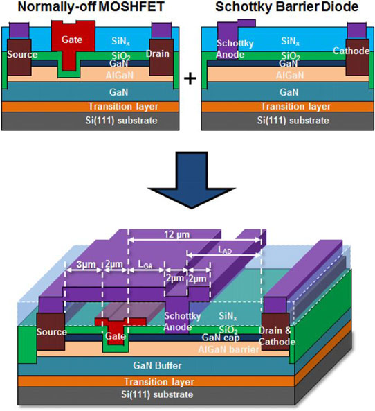
Figure 1: Cross-sectional schematic of SBD embedded AlGaN/GaN-on-Si switching transistor.
Mesa isolation was performed with an inductively coupled plasma reactive-ion etch (ICP-RIE). This was followed by gate recess patterning and further ICP-RIE. The recess into the AlGaN barrier had a target AlGaN thickness between the gate foot and GaN buffer of 3nm. The recessing has to be this thin in order for the channel to be completely depleted under the gate, giving normally-off behavior.
Next, a 35nm layer of silicon dioxide was applied using ICP chemical vapor deposition (ICP-CVD). This layer was then patterned and openings made for the ohmic contacts with ICP-RIE. The ohmic metals consisted of silicon/titanium/aluminium/molybdenum/gold annealed at 820°C in nitrogen for 30 seconds. The gate electrode consisted of nickel/gold.
The Schottky barrier diode was created with ICP-CVD of silicon nitride insulation and ICP-RIE/wet buffered oxide etch (BOE) of the anode contact region. The remaining metallization was nickel/gold. The main variable in the devices was the anode-drain distance (LAD) with the related gate-anode distance (LGA), being 10μm - LAD.
The Hongik/Cornell device acts as a normally-off transistor with forward drain bias (Figure 2). The diode blocks current flow. However, with negative drain bias sufficient to turn on the Schottky diode (-1.2V), current flows even when the transistor is off (0V gate) through the anode contact and over through a field-plate structure attached to the source terminal. With the transistor on with a negative drain bias, current flows through both the transistor and the diode structure.
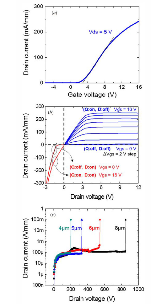
Figure 2: (a) Transfer and (b) drain current–voltage characteristics of the anode-to-drain distance of 8μm and (c) breakdown characteristics of fabricated devices as a function of anode-to-drain distance (LAD).
The maximum forward current was 252mA/mm at 16V gate potential. The on-resistance was 2.66Ω-cm2. The transistor threshold was estimated at +2.8V.
The researchers point out that a significant difference from GIT-type devices is that the Schottky diode turn-on voltage is not affected by the gate potential. This gives an extra degree of freedom for device design. Variations in fabrication such as recess depth and gate dielectric could change the threshold, while the Schottky turn-on could be altered by removing the GaN cap under the anode and/or by changing the metals used.
Off-state breakdown was found for 0V gate as a function of the anode-drain distance. With an LAD of 8μm, breakdown set in at 849V drain bias. The researchers say that breakdown is governed by the SBD, not the HEMT. Hence, shorter LAD values give lower breakdown voltages.
The researchers speculate that the high leakage current level of ~100μA/mm (0.1mA/mm) in the off-state was due to buffer leakage, which could be improved by optimization of buffer quality and better mesa isolation.
The impact of high temperature (up to 300°C) on device performance was also investigated on devices with LAD of 4μm. The transistor threshold showed no noticeable change. However, the on-currents in both the transistor and diode tend to degrade at elevated temperature. Enhanced thermionic emission also means that the diode turn-on voltage ‘decreases’ slightly – i.e. it turns on sooner with negative drain bias of the device.
GaN transistors MOSHEMT Schottky barrier diode ICP-RIE ICP-CVD AlGaN
http://iopscience.iop.org/0268-1242/28/12/125003/
The author Mike Cooke is a freelance technology journalist who has worked in the semiconductor and advanced technology sectors since 1997.


