


- News
5 November 2013
LayTec’s EpiCurve TT improves HVPE GaN growth at Ulm university
LayTec AG of Berlin, Germany, which makes in-situ metrology systems for thin-film processes, focusing on compound semiconductor and photovoltaic applications, says that researchers at Germany’s Ulm University have used LayTec’s EpiCurve TT in-situ system in their work on growing think (1 mm and more) gallium nitride (GaN) layers using hydride vapor phase epitaxy (HVPE).
A major challenge to growing thick GaN layers by HVPE is the bowing of the free-standing GaN after its self separation from the sapphire substrate. Martin Klein and his colleagues at Ulm University have proved that the initial strain of the MOVPE template has a great impact on the final bowing of HVPE samples and on the remaining curvature of separated GaN wafers. See: M. Klein in Annual Report 2012, University of Ulm, pp. 83-90 - www.uni-ulm.de/in/opto/forschung/jahresberichte.html
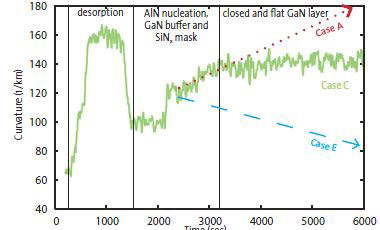 Figure 1: In-situ curvature measurements during MOVPE template growth on sapphire. A, C, E correlate to Figure 2.
To optimize the template conditions, the researchers used in their MOVPE process a combination of an oxygen doped AlN nucleation layer, GaN buffer and a sub-monolayer of SiNx mask. With LayTec’s EpiCurve TT, they monitored the related curvature changes during growth (Figure: 1). By variations of the growth conditions of the AlN nucleation and the subsequent GaN buffer layer, the curvature of the templates could be varied between tensile and compressive strain. Under optimized conditions, a fairly flat template could be produced (Case C), thereby being optimized for the subsequent HVPE growth.
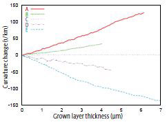 Figure 2: In-situ curvature data during overgrowth in HVPE. Lines A–E: identical growth runs on
different templates.
Figure 2 shows EpiCurve TT measurements during the subsequent HVPE growth. Lines A, C, E refer to the related template procedures in Figure 1. B and D relate to intermediate AlN buffer thickness. All samples showed the same HVPE curvature evolution as their MOCVD templates. In the end, the final separated GaN layers grown on optimized C-type templates had low curvature values (100-200 km-1) regardless of their thickness.
As the next step, applying their newly acquired understanding of the MOCVD/HVPE strain effects, researchers in Ulm plan to use pre-curved sapphire wafers as templates to produce GaN wafers with zero bow.


