


- News
18 November 2013
Hole conductivity in zinc sulfide telluride and blue-green light emission
Japan’s Tottori University has produced blue-green light-emitting diode (LED) structures using zinc sulfide telluride (ZnSTe) material [Kunio Ichino et al, Appl. Phys. Express, vol6, p112102, 2013]. The researchers see their work as rather preliminary, with the importance being “that the results suggest p-type conductivity of the ZnSTe:N layer and the formation of a ZnS-based pn junction.”
Zinc sulfide is a material with a wide energy bandgap of 3.73eV that would promise ultraviolet optical applications if a convenient method could be found to produce hole/p-type conductivity. Although there have been reports of p-ZnS, no light-emitting devices based on ZnS pn junctions have been demonstrated. Previously reported ZnS light emission is likely due to metal-insulator-semiconductor structuring.
Zinc telluride has a narrower gap of 2.26eV and is naturally p-type/hole conducting. The p-type conductivity can be enhanced to hole concentrations of 1019/cm2 by doping with nitrogen. Hence the investigation of ZnSTe as a medium for p-type conductivity would seem promising.
The diode structures were grown on (001) gallium phosphide (GaP) substrates using 275°C molecular beam epitaxy (MBE) – see Figure 1. The layers consisted of a 1.5μm chlorine-doped zinc sulfide (n-ZnS:Cl) buffer and 2.5μm nitrogen-doped zinc sulfide telluride (ZnSTe:N) with telluride fractions up to 30%. The n-ZnS carrier density was estimated at 1017/cm3.
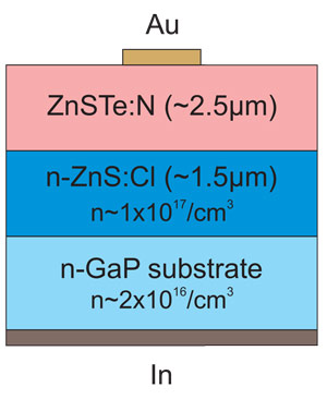 Figure 1: Schematic of Au/ZnS1-xTex:N/n-ZnS/n-GaP diode structure.
The substrates were supplied by Shin-Etsu Chemical and Sumitomo Metal Mining. The Shin-Etsu product was not intentionally doped, but had an electron carrier (n-type) concentration of 2x10¹⁶/cm3. The Sumitomo substrate was semi-insulating.
The MBE sources were zinc and tellurium metals (Osaka Asahi Metal) and elemental sulfur (Furukawa Denshi). The nitrogen doping was achieved using radio frequency plasma generated from nitrogen gas (EIKO). The chlorine source was zinc chloride.
The growth process took account of the fact that sulfur is preferentially incorporated, compared with tellurium. In particular the sulfur flux was reduced to decrease the evaporation temperature from 155°C to 110°C. The tellurium flux was simultaneously varied to deliver different compositions.
After material growth, gold (Au) and indium contacts were added to the top ZnSTe:N layer and bottom n-GaP substrate, respectively. A 5mm x 8mm chip with 15% Te-fraction in the top layer showed clear rectifying behavior with significant current flow only when the top gold p-contact was positively biased. A diode without N-doping of the top ZnSTe layer showed almost no current flow under positive or negative bias.
The researchers comment: “The polarity of the rectification can be due to either an Au/n-ZnS(Te) Schottky contact in such a case that the ZnSTe layer is n-type or highly resistive, or a p-ZnSTe/n-ZnS junction when the ZnSTe layer is p-type. Since the Au/ZnS1-xTex:N contact has been found to be ohmic [. . .] the latter is probable.”
Although attempts by the researchers to determine p-type behavior of ZnSTe:N layers by Hall effect measurements with a different material structure were impeded by the voltage being too low to be detected, electron-beam-induced current (EBIC) analysis of the LED structure using a scanning electron microscope (SEM) found a peak at the ZnSTe:N/n-ZnS interface. “This means that a depletion layer, or an internal electric field exists at the ZnSTe:N/n-ZnS interface, and suggests that the ZnSTe:N layer is p-type,” they write.
The performance of devices with Te fractions away from 15% were found to be degraded. SEM analysis also showed deterioration in crystal quality in all ZnSTe:N structures as growth proceeds.
Although electroluminescence was visible to the naked eye (Figure 2), the researchers say that the optical power and efficiency were too low for practical use. Because the spectral analysis shows broad peaks, the researchers suggest that the light comes from hole injection into the n-ZnS giving self-activated deep-level, rather than band-edge, emission. It seems that electrons injected in the other direction recombine with holes without emitting light. At 10mA, the forward voltage was 30V.
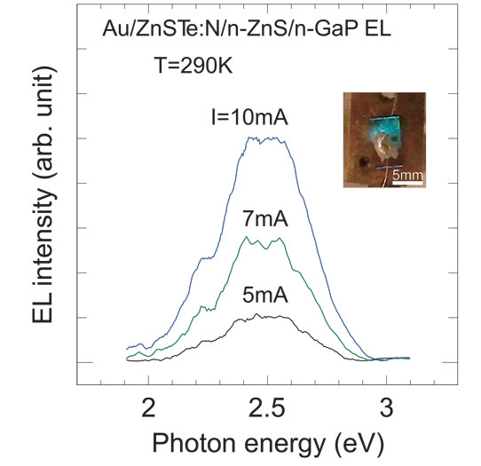
Figure 2: Electroluminescence (EL) spectra of ZnS0.85Te0.15:N/n-ZnS diode structure under forward current (I) of 5mA, 7mA and 10mA at 290K. (Photon energy 2.5eV corresponds to a 496nm wavelength.) Inset: EL image (I = 10mA). The silver paste bonding a gold wire overlays three top gold contacts in this device.
There is a ‘threshold’ for light emission of about 4mA. The threshold behavior is seen as being consistent with electron injection into the ZnSTe:N dominating at small bias. “When the forward bias is further increased, the electric field would be concentrated at the interface high-resistivity layer, and at a certain point the hole injection from the ZnSTe:N layer into the n-ZnS layer would start to occur, giving rise to the EL emission,” the researchers add.
http://apex.jsap.jp/link?APEX/6/112102/
The author Mike Cooke is a freelance technology journalist who has worked in the semiconductor and advanced technology sectors since 1997.


