


- News
22 November 2013
Semipolar nitride laser diodes without AlGaN cladding
University of California Santa Barbara (UCSB) has developed semipolar (20-2-1) nitride semiconductor laser diodes (LDs) without using aluminium gallium nitride (AlGaN) as the cladding material for optical confinement [A. Pourhashemi et al, Appl. Phys. Lett., vol103, p151112, 2013].
The use of AlGaN in polar c-plane laser diodes creates a highly confined and intense optical field that is subject to failure through catastrophic optical mirror damage (COMD). One reason for the use of AlGaN with c-plane devices is the need to keep the structures thin enough to accommodate the effects of polarization-related electric fields.
In semipolar devices these electric fields are less strong and the structures do not have to be so thin. Thicker cladding regions based on other nitride semiconductor material structures could reduce the optical field intensity and delay COMD. Semipolar devices are also being developed on the basis that the reduced polarization-related electric fields could also lead to more efficient light emission.
The UCSB team also believes that improving the efficiency of blue and ultraviolet nitride semiconductor laser diodes could lead to laser-based white lighting systems, avoiding the problem of efficiency droop at high current in GaN-based light-emitting diodes (LEDs) [see, for example, White light from near-UV and blue laser diodes and phosphors].
Mitsubishi Chemical Corp supplied the semipolar (20-2-1) gallium nitride (GaN) substrates that UCSB used to create the LD epitaxial structures (Figure 1) through metal-organic chemical vapor deposition (MOCVD). The p-type GaN layers had a varying doping profile from very low (p--) to high (p+) in the thin contact layer. This was to avoid absorption losses by moving the high doping region far away from the optical fields.
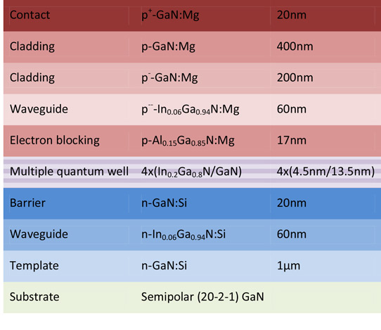
Figure 1: Schematic for laser diode epitaxial structure.
Simulations on the structure suggest a transverse confinement factor of 4.7% from the relatively wide active region and the indium gallium nitride/gallium nitride (In0.06Ga0.94N/GaN) waveguide/cladding separate-confinement heterostructures (SCH).
UCSB used the epitaxial material to make 8μm x 900μm ridge waveguide laser diodes through reactive ion etch. Then silicon dioxide was applied to the sides of the ridges and the surrounding areas as insulation. The p- and n-electrodes consisted of palladium/gold and aluminium/gold, respectively.
The facets were created using a dicing saw and mechanical polishing. A highly reflective coating of eight alternating quarter-wavelength layers of silicon dioxide (SiO2) and tantalum pentoxide (Ta2O5) was applied to the back facet. An anti-reflective coating for the front facet consisted of a single period of SiO2/Ta2O5 quarter-wavelength layers.
The performance of the laser diodes was characterized under pulsed drive currents (Figure 2a). The light output power showed a lasing threshold at 392mA current (5.30kA/cm2 density). The slope efficiency was 1.35W/A, corresponding to a differential efficiency of 49%. The maximum output power was 2.15W at 2.02A (28.1kA/cm2).
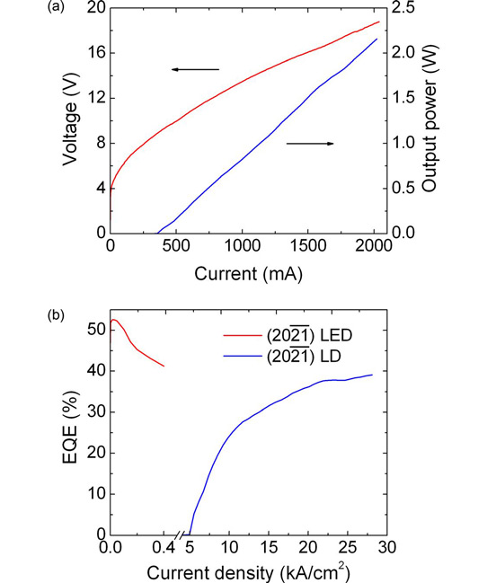
Figure 2: (a) Light output power–current–voltage (L–I–V) characteristics of UCSB LD. (b) Comparison of EQE for UCSB’s blue (~460nm wavelength) semipolar (20-2-1) LD with a blue semipolar (20-2-1) LED.
The researchers estimate that peak optical power density at the front facet was 70.2MW/cm2. This is similar to the values causing COMD in high power c-plane InGaN/GaN LDs (40-70MW/cm2). COMD occurs at lower power densities of ~30MW/cm2 in gallium arsenide laser diodes.
In fact, the limitation for the UCSB device was not thermal degradation (‘roll-over’) or COMD, but rather the inability of the power supply to give currents above 2.02A.
The external quantum efficiency (EQE) actually increases with increasing current, reaching 39% at 2.02A. This is very unlike the case for light-emitting diodes where ‘efficiency droop’ typically occurs after a few tens of milliamps.
The researchers comment: “This marked difference in behavior can be explained by the clamping of the carrier density that occurs in a LD above threshold, which in turn clamps nonradiative recombination processes and eliminates efficiency droop above threshold.”
The researchers compared the EQE performance (Figure 2b) with a blue (20-2-1) LED that reaches a peak EQE of ~40%. The laser diode reaches 39% EQE at a current density that is 75 times that of the peak EQE of the LED.
The threshold voltage of 9V was “rather high”, compared with other semipolar LDs, according to the researchers. The series resistance after turn-on was 6Ω. At maximum power output of 2.15W, the voltage was 18.7V. This high operating voltage cuts wall-plug efficiency, despite the high EQE, “limiting the usefulness of such LDs in practical applications”.
The researchers report that they are investigating the source of the high series resistance, and experiments in progress indicate that the major contributor is the p-contact region. The team therefore believes that optimizing the p-contact region should give a “marked reduction on the overall operating voltage”.
Measurements between 20°C and 80°C gave an exponential increase in threshold current that is described by a characteristic temperature of 91K.
Laser diodes GaN substrates MOCVD
http://dx.doi.org/10.1063/1.4824773
The author Mike Cooke is a freelance technology journalist who has worked in the semiconductor and advanced technology sectors since 1997.


