


- News
28 October 2013
Lateral current thinking improves light and voltage in nitride LEDs
LG Electronics Materials and Components Laboratory in South Korea has used aluminium gallium nitride (AlGaN) superlattice structures (SLs) to improve lateral current spreading from the n-side of nitride semiconductor light-emitting diodes (LEDs) [Hooyoung Song et al, Appl. Phys. Lett., vol103, p141102, 2013].
Lateral current spreading is important in nitride semiconductor LEDs for several reasons. For example, these devices are mostly produced with the n-contact to one side of the LED because vertical flow is not possible through insulating substrates such as sapphire. Also, nitride semiconductor LEDs suffer from efficiency droop effects at high current density so that non-uniform flow through the devices leads to avoidable power losses.
Superlattice structures have previously been used to improve current flow properties of nitride LEDs from the p-side because hole generation and flow are often seen as stumbling blocks on the path to more efficient LEDs. “However,” the LG researchers say, “n-type conductivity is also an important factor in devices such as LEDs where current spreading still remains as an issue.” They thus set out to investigate “methods to enhance transport properties of n-type AlGaN/GaN SLs layers and demonstrate improved LED performance from n-type AlGaN/GaN SLs embedded LED structures”.
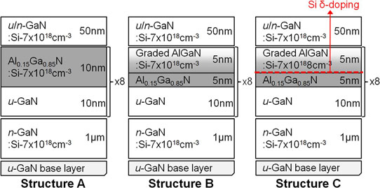
Figure 1: Schematics of structures A, B and C used to explore current-spreading effects of superlattices.
The nitride structures were grown using metal-organic chemical vapor deposition (MOCVD). Various current-spreading AlGaN/GaN superlattices were produced based on simulations (Figure 1). These structures were tested using Hall-effect measurements and by incorporation into LEDs (Figure 2). Standard lateral LEDs were fabricated with mesa etch, and the application of indium tin oxide (ITO) transparent conductor on the p-GaN top layer and chromium/nickel/gold n- and p-electrodes.
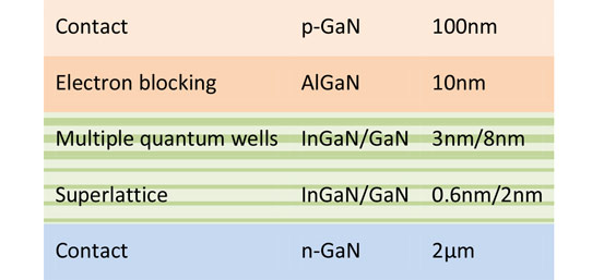
Figure 2: Schematic of LED layers. Where there was an AlGaN/GaN superlattice (structures A-C), this was 1μm below the InGaN/GaN superlattice.
The Hall-effect measurements (Table 1) showed improved conductivity for the superlattices over a 1.2μm n-GaN layer with target doping concentration of 7x10¹⁸/cm3 (“structure D”). The higher mobility of the superlattice structures ‘B’ and ‘C’ was attributed to “reduced ionized impurity scattering as a result of undoped AlGaN layer that separates 2DEG channel and Si-doped graded AlGaN layer”.
Table 1: Hall-effect measurements for structure A, B, C, and D.
| Sample | Sheet concentration (x1013/cm2 | Mobility (cm2/V-s) | Conductivity (/Ω-cm) |
| Structure A | 6.61 | 649 | 289 |
| Structure B | 6.25 | 960 | 340 |
| Structure C | 1.02 | 1075 | 569 |
| Structure D | N/A | 237 | 197 |
In addition to lateral conductivity, superlattices for use with LED structures need to have good vertical conductivity. Tests of the vertical conductivity of the superlattices were in line with simulations with high conductivity correlated with low barrier height. Thus, structure C had a similar vertical conductivity to the reference structure D. By contrast, structures A and B had reduced current for a given voltage, with the lowest vertical current being that through structure A that had the highest barriers in simulation.
The performance of the LEDs (Figure 3) confirmed the superiority of structure C for giving improved current spreading without impacting the vertical flow. The peak wavelength at 60A/cm2 current density was 635nm for all devices. At the same current, the output powers were 73.1mW, 75.3mW, 79.9mW, and 70.1mW for structure A-D, respectively.
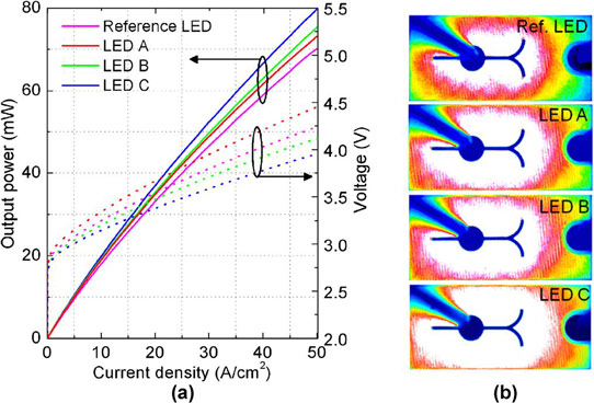
Figure 3: (a) Output power-current-voltage (L-I-V) relations and (b) current-spreading images of LED A, B, C, and reference.
The devices with current-spreading superlattices showed increased output power. However, structure A with high barriers to vertical current flow also showed the highest forward voltage, indicating series resistance.
The structure C LED had 13.7% better light output power and 6.7% reduced forward voltage at 60A/cm2, compared with the reference LED (structure D).
AlGaN superlattice structures Nitride LEDs MOCVD
http://dx.doi.org/10.1063/1.4823507
The author Mike Cooke is a freelance technology journalist who has worked in the semiconductor and advanced technology sectors since 1997.


