


- News
7 October 2013
Growth switching for higher-efficiency near-green indium gallium nitride LEDs
Taiwan’s National Cheng Kung University has developed near-green light-emitting diodes (LEDs) using a new indium gallium nitride (InGaN) growth process that gives devices with a higher peak external quantum efficiency of 48.6% [Wei-Chih Lai et al, Appl. Phys. Express, vol6, p102101, 2013]. The process involves switching the growth between indium nitride and gallium nitride in 2-second bursts.
Many researchers are seeking to improve the efficiency of green LEDs. At present there are no ideal materials for producing efficient LEDs for the yellow-green gap in the visible spectrum between the red-orange of arsenide- and phosphide-based devices and the blue of indium gallium nitride.
The LED material (Figure 1) was grown on patterned sapphire in a Thomas Swan 19x2-inch close coupled showerhead (CCS) metal-organic chemical vapor deposition (MOCVD) system. The CCS technology is now owned by Aixtron. The sapphire patterning consisted of an array of 3.5μm-diameter cones with 2μm spacing. The height of the cones was 1.3μm.
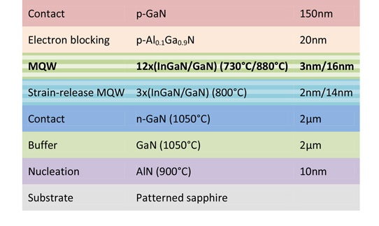
Figure 1: General structure of LEDs.
The nitride semiconductor metal-organic epitaxy sources were trimethyl-gallium, indium and aluminium (TMG, TMI, TMA), along with ammonia (NH3) for the nitrogen. The InN/GaN switching (Figure 2) was performed in the active light-emitting region multiple quantum well (MQW). The switching loop consisted of 40 cycles of 2 second bursts of TMG and TMI. The ammonia flow was held constant. The researchers also produced a standard MQW (LED I) with constant flow of TMG and TMI during the well growth.
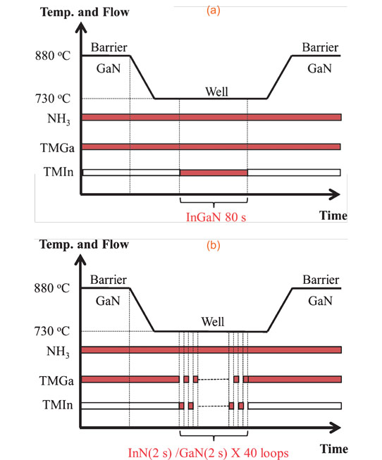
Figure 2: Schematic of source switching sequences of MQW growth of LEDs: (a) I and (b) II.
LEDs with a photoluminescence (PL) emission wavelength of 516nm were created. The chip area was 580μm x 1160μm. The LEDs included an indium tin oxide (ITO) transparent conducting electrode.
X-ray and PL analysis of the epitaxial material suggested that the switched InN/GaN well growth (LED II) gives better crystal quality. The PL full-width at half-maximum (FWHM) for LED II was 24.6nm, compared with 29.1nm for LED I. The x-ray θ-2θ diffraction -1-order satellite peak also showed a narrowing for LED II: 89arcsec compared with 93.5arcsec. Broader satellite peaks are associated with increased interface roughness or fluctuations in alloy composition.
Under current injection of 120mA, the forward voltage of LED I was 3.35V and slightly less at 3.34V for LED II. The reverse leakage current at -15V was 53.7μA for LED I and 5.1μA for LED II. The shape of the current-voltage curve, as measured by the ‘ideality factor’, suggested reduced non-radiative recombination for LED II. Non-radiative recombination reduces the efficiency of light emission.
The researchers believe that the better ideality factor and reduced reverse current leakage could be attributed to improved crystal quality for green InGaN/GaN MQWs from LED II’s switched InN/GaN growth process.
The electroluminescence (EL) light output power and external quantum efficiency (EQE) data confirm the expectations from the ideality factor and reverse current leakage (Figure 3). At 120mA, the light output powers are 89.5mW and 110.2mW for LEDs I and II, respectively. The respective EQEs are 30.8% and 37.9%. The peak EQE values are 48.6% for LED II and 34.0% for LED I.
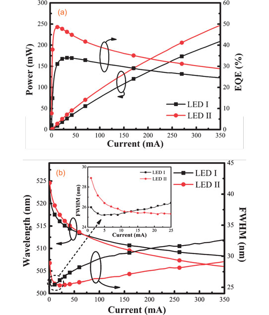
Figure 3: (a) Light output power, EQE, and (b) current-dependent emission wavelength and FWHM of LEDs I and II.
One disappointing feature of LED II was a faster efficiency droop at 350mA of 44.6% from the peak value. The corresponding droop for LED I was 30.7%.
The researchers also studied the blue-shift and FWHM of the EL emission spectrum. This study suggested that the improved crystal quality of LED II may have increased the strain-induced polarization field and thus would lead to a stronger quantum-confined Stark effect (QCSE) where the electrons and holes are pulled apart by large electric fields, reducing light emission. The researchers comment that this would “result in LED II having a larger emission wavelength blue-shift and efficiency drop than LED I”.
LEDs Near-green LEDs InGaN MOCVD
http://apex.jsap.jp/link?APEX/6/102101
The author Mike Cooke is a freelance technology journalist who has worked in the semiconductor and advanced technology sectors since 1997.


