


- News
11 October 2013
High-frequency nitride HEMTs on silicon with high breakdown
Singapore’s Nanyang Technological University (NTU) has developed a passivation process for aluminium gallium nitride on gallium nitride (AlGaN/GaN) high-electron-mobility transistors (HEMTs) on silicon substrates that significantly improves breakdown voltage without impacting frequency performance [S. Arulkumaran et al, IEEE Electron Device Letters, 16 September 2013].
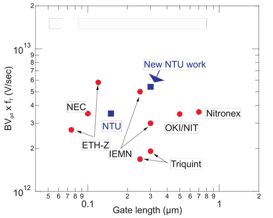
Figure 1: State-of-the-art Johnson figures of merit versus gate lengths for AlGaN/GaN HEMTs on silicon substrates.
The Johnson figure of merit combining breakdown voltage and cut-off frequency (BVgd x fT) was 5.41 x10¹²V/sec (Figure 1, Table 1), “which is the highest value reported so far for 0.3μm T-gate conventional SiN passivated AlGaN/GaN HEMTs on Si substrate without additional Γ-gate and/or source field plate.”
Table 1: State-of-the-art fT and BVgd for conventional AlGaN/GaN HEMTS on Si.
| fT (GHz) | BVgd (V) | BVgd x fT (x1012V/s) | Gate type | Passivation | |
| IEMN | 50.0 | 100 | 5.00 | T-gate | SiO2/SiN |
| OKI/NIT | 13.9 | 250 | 3.48 | Γ-gate & SFP | SiN |
| ETH-Z | 100.0 | 58 | 5.80 | T-gate | SiN |
| NTU | 39.0 | 90 | 3.51 | T-gate (non-gold) | SiN |
| Triquint | 24.0 | 70 | 1.68 | T-gate & SFP | SiN |
| Nitronex | 18.0 | 200 | 3.60 | Γ-gate & SFP | SiN |
| NEC | 60.0 | 55 | 3.30 | T-gate | SiN |
| NTU treated HEMT | 34.0 | 159 | 5.41 | T-gate | [(NH4)2Sx] + SiN |
The AlGaN/GaN semiconductor layers (Figure 2) were applied to 4-inch high-resistivity (more than 6000Ω-cm) silicon substrates using metal-organic chemical vapor deposition (MOCVD). The mobility and carrier density of the two-dimensional electron gas (2DEG) channel were 1455cm2/V-s and 9.6x10¹²/cm2, respectively.
Transistor fabrication began with plasma etch of the mesa isolation, and application and annealing of titanium/aluminium/nickel/gold ohmic source-drain electrodes.
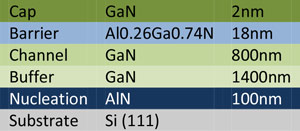 Figure 2: Schematic structure of nitride semiconductor epitaxy on silicon for HEMT.
Preparation for the silicon nitride passivation consisted of a 1-minute buffer hydrofluoric acid dip, and an ammonium sulfide ((NH4)2Sx) surface treatment at 50°C for 15 minutes. The silicon nitride was applied in a 50nm layer using plasma-enhanced chemical vapor deposition (PECVD at 300°C).
Gate formation consisted of electron-beam patterning and silicon nitride etch. The gate footprint was 0.3μm and the gate head was 0.7μm. The gate stack consisted of 50nm of nickel and 400nm of gold.
Final processing consisted of adding titanium/gold (50nm/1000nm) transmission lines and further passivation with 150nm of PECVD silicon nitride.
Comparison devices were also produced without the (NH4)2Sx) surface treatment.
The maximum drain current of the treated device was 646mA/mm, compared with 636mA/mm for the untreated HEMT. The respective peak extrinsic transconductances were 175mS/mm and 205mS/mm. A real difference in performance is seen in the on/off current ratios, which are three orders of magnitude higher in the treated HEMT.
Another improvement is the much lower subthreshold swing of the treated device: 77mV/decade, compared with 112mV/dec for the untreated device. The researchers consider the low subthreshold swing to be evidence of low interface trap densities as a result of the (NH4)2Sx surface treatment.
A further benefit of treatment is a six-fold increase in gate-drain breakdown voltage (BVgd for drain current 0.5mA/mm) to 159V. The higher breakdown voltage was achieved while maintaining a cut-off frequency (fT) of 34GHz and maximum oscillation (fmax) of 52GHz. The cut-off gate-length product (fT x Lg) was 10.2GHz-μm, which is a little smaller than the best value of 12.5GHz-μm reported in 2005 by Lille University.
The researchers found that the improved breakdown performance is linked to three orders of magnitude lower surface current leakage in the treated devices by passivation of dangling bonds and interface traps between GaN and SiN.
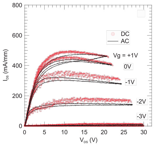
Figure 3: DC and AC (100Hz) drain current versus drain voltage characteristics of AlGaN/GaN HEMTs (Lsg/Wg/Lg/Lgd = 1.0/(2x100)/0.3/3.0μm).
The researchers also carried out 100Hz AC measurements, which showed “no significant drain current collapse” (Figure 3).
Nitride HEMTs on silicon AlGaN GaN Silicon substrates MOCVD
http://ieeexplore.ieee.org/xpl/articleDetails.jsp?arnumber=6600863
The author Mike Cooke is a freelance technology journalist who has worked in the semiconductor and advanced technology sectors since 1997.


