


- News
26 September 2013
Azzurro boosts nitride LED on silicon uniformity with strain engineering
Germany’s Azzurro Semiconductors AG has reported uniformity measurements for indium gallium nitride (InGaN) light-emitting diodes on large-diameter silicon substrates up to 200mm [Andrea Pinos, etal, Appl. Phys. Express, vol6, p095502, 2013].
Although the growth of nitride semiconductor LEDs on larger substrates should provide economies of scale, there remain a number of production challenges to overcome before a commercial process can be developed. Among these challenges is the processing of high-quality, reliable material that gives uniform performance across the wafer.
An obvious roadblock is the 17% mismatch in lattice spacing between silicon and gallium nitride (GaN). This is higher than alternative but more expensive (and only available in smaller size) substrates such as sapphire (16%) or silicon carbide (3%). Further, since the GaN growth process involves a raised temperate (~1000°C is typical), the 46% mismatch in the thermal expansion coefficients raises an even more serious obstacle.
Both the lattice and thermal expansion mismatches can lead to significant wafer bowing and even cracking of the semiconductor material. It is not surprising therefore that nitride LEDs grown on silicon can show large variations in performance and yield across the wafer.
Azzurro has developed a proprietary process that results in a strain-engineered buffer layer that avoids the problems of lattice and thermal expansion mismatches. Judging from the company’s previously published research [e.g. Atsushi Nishikawa et al, Jpn. J. Appl. Phys., vol52, p08JB25, 2013], the process involves bridging layers of aluminium gallium nitride (AlGaN) and aluminium nitride (AlN).
The LED material was grown on (111) silicon substrates using multi-wafer metal-organic chemical vapor deposition (MOCVD). On top of the GaN template further layers consisted of 2μm of silicon-doped n-GaN buffer, the LED active region, and magnesium-doped p-GaN contact.
For simple testing, electrical contact with the LED structures was through 400nm annealed indium tin oxide (ITO) on the p-GaN with 150μm-diameter platinum/aluminium bond pads, and a conductive vacuum chuck on which the conductive silicon substrate was placed.
Since silicon absorbs the frequency emitted by the LED structures, one would normally remove the substrate for commercial products. Also, the devices were not etched to provide mesa isolation.
A range of uniformity measurements were carried out for 150mm-diameter wafers (Table 1). Also, the electroluminescence (EL) peak wavelength for LEDs on 200mm wafers was 447nm on average with 3.72nm standard deviation, representing 0.8% uniformity.
Table 1: Uniformity performance of LEDs on 150mm silicon substrate.
| 350mA EL peak average ± standard deviation (nm) | 447±2.79 (0.6%) |
| PL peak average ± standard deviation (nm) | 455.6±3.433 (0.754%) |
| 350mA EL intensity average ± standard deviation (mW) | 15.7±0.61 (3.9%) |
| PL intensity average ± standard deviation (a.u.) | 677.4±123.3 (18.2%) |
| 5mA forward voltage (V) | 3.1±0.04 (1.3%) |
The standard deviation values for the EL peak wavelength on 150mm and 200mm wafers are claimed to be among the lowest reported to date (Figure 1). The researchers comment: “Achieving good wavelength uniformity on LED epitaxial wafers has been one of the main topics discussed in the US DOE SSL Manufacturing Roadmap and a key parameter to reducing manufacturing costs.”
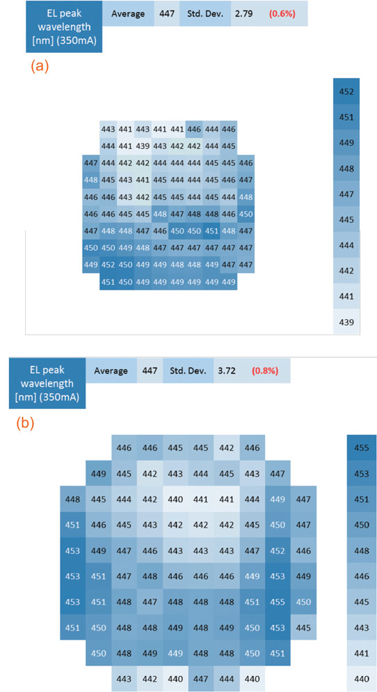
Figure 1: EL peak wavelength measured at 350mA on (a) 150mm and (b) 200mm wafers. The relative dimensions of the two maps reflect the different substrate areas.
The photoluminescence (PL) spectra show a yellow band with an intensity two orders of magnitude lower than the main band-to-band emission. The EL spectra do not show such a yellow band. The researchers comment that yellow emissions are often associated with carbon-related levels from the organic precursors.
The EL intensity (Figure 2) standard deviation of 0.61 represents a relative variation of 3.9%, which is the best value reported so far for LEDs on large-diameter substrates according to the researchers.
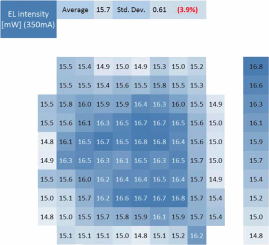
Figure 2: On-wafer EL intensity for 150mm wafer at 350mA.
The relatively high value of the forward voltage at 5mA and the implied high series resistance is blamed on the AlGaN/AlN buffer layers between the n-Si and n-GaN. The researchers point out that these layers would be removed in a commercial process.
The researchers comment: “These results are significant, as the simultaneous demonstration of uniform EL intensity, wavelength and forward voltage clearly suggests that very uniform quantum wells can be achieved by MOCVD on large-area Si substrates when proper strain engineering is applied. This translates to a reduced binning and a higher manufacturing yield, in addition to cost savings from a reduced testing overhead from fewer bins.”
The researchers also studied the reverse-bias leakage current variation with temperature and voltage. The strong temperature dependence that the researchers found suggests that “minimization of the dislocation density is critical for improving the LED brightness and reliability.”
Azzurro InGaN Silicon substrates LEDs MOCVD
http://apex.jsap.jp/link?APEX/6/095502/
The author Mike Cooke is a freelance technology journalist who has worked in the semiconductor and advanced technology sectors since 1997.
