


- News
18 September 2013
Imec, KULeuven and AIST report process paving way to increased mobility of beyond-10nm MOS
KULeuven (Katholieke Universiteit Leuven), nanoelectronics research center Imec of Leuven, Belgium and the National Institute of Advanced Industrial Science and Technology (AIST) of Tsukuba, Japan have developed a solid-phase epitaxy process to integrate germanium-tin (GeSn) metal-oxide semiconductor field-effect transistor (MOSFET) devices on silicon. For the first time, it is claimed, operation of a depletion-mode junctionless GeSn pMOSFET on silicon was demonstrated (a key step toward achieving tensile strain in MOSFET devices, and increasing their mobility).
To improve performance in next-generation scaled complementary metal-oxide semiconductor (CMOS) devices, researchers are exploring the integration of novel materials with superior electron mobility. This includes GeSn, a promising semiconductor candidate for the channel material, due to its superior physical properties. GeSn enables increased switching speed of MOSFET devices and can be used in fast optical communication. While most prototype GeSn-channel MOSFETs are fabricated on Ge substrates, silicon integration is preferred for CMOS compatibility.
However, epitaxial growth of GeSn on silicon substrates poses several challenges, including limited solubility of Sn in Ge (0.5%), its compositional fluctuations, Sn segregation, and large lattice mismatch (>4%). It is hence critical to suppress these effects to obtain high-performance devices with GeSn layers.
Researchers at KULeuven, imec and AIST developed a solid-phase epitaxy process, achieving ultra-thin (~10nm) single-crystalline GeSn layers on silicon substrates showing tensile strain, which is attractive for strain engineering of Ge channels. Furthermore, it reduces the difference between the direct and indirect band transition, resulting in a direct-bandgap group IV material. Lastly, due to its non-equilibrium deposition conditions, the new method enables the development of GeSn with high Sn concentrations.
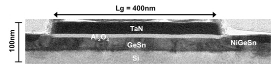
Picture: TEM image of NiGeSn metal S/D MOSFET, observed along [11-2]: the channel direction is [-110] and the surface orientation is (111).
By decreasing the channel thickness with reactive ion etching (RIE) from ~30 to ~10nm, the researchers improved the on/off ratio by more than one order of magnitude. Additionally, hole depletion in the ultra-thin (~10nm) GeSn layers on silicon resulted in good transfer characteristics with an on/off ratio of 84. In the future, research will focus on optimizing the GeSn MOSFET on silicon devices to further increase the channel mobility.
More details on these results are being presented on 25 September at the 45th International Conference on Solid State Devices and Materials (SSDM 2013) in Fukuoka, Japan, and will be published in Applied Physics Express.
