


- News
13 September 2013
Increasing output power from nitride LEDs with p-InGaN contacts
Jimei University in China has used indium gallium nitride (InGaN) p-type contacts to increase light output power by 45% over a reference device [Wang Min-Shuai and Huang Xiao-Jing, Chin. Phys. B, vol. 22, p086803, 2013].
The researchers believe that the most important factor for the improved performance of the p-InGaN LED was reduced activation energy, creating an increased hole density. The team estimates that the activation energy was reduced from 180-200meV for normal p-GaN contacts to 50meV-100meV (or even 43meV!) for the p-InGaN, leading to a hole density around 5x10¹⁸/cm3.
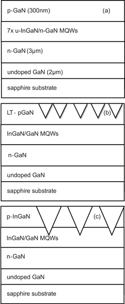 Figure 1. Schematic diagram of GaN-based LED structures with Ref-LED (a), LT p-GaN LED (b), and p-InGaN LED (c).
A by-product of the growth process for the p-InGaN is that V-shaped pits appear on the surface. Normal flat p-GaN surfaces tend to reduce light extraction efficiency because the difference in refractive index with that of air reduces the escape cone to around 23°. The V-pits in the p-InGaN are also thought to improve the light output from the p-InGaN devices due to secondary factors such as an increased contact area and increased light extraction from the textured surface.
Other researchers have tried increasing light extraction in p-GaN by deliberately introducing V-pits by using a reduced-temperature growth process. However, these devices suffer from poor activation of the magnesium (Mg) p-type dopant, leading to reduced hole densities and thus the creation of a high-resistance contact that wastes power.
Nitride semiconductor structures for the Jimei 460nm blue LEDs (Figure 1) were grown on c-plane sapphire substrates using low-pressure metal-organic chemical vapor deposition (MOCVD). The top p-type contact layer included an aluminium gallium nitride (p-AlGaN) electron-blocking layer before the 300nm p-GaN. The p-type magnesium doping was activated with a 10-minute 600°C anneal in air.
LED fabrication included deposition of an indium tin oxide (ITO) transparent contact/current spreading layer, and chromium/gold electrodes on the n- and p-contacts.
LEDs with V-shaped pits were formed in two different processes. First, a low-temperature (LT) 820°C process was used to deposit p-GaN (Figure 1b), rather than the 920°C used to give a planar p-GaN reference device (Figure 1a). The other V-shaped pit LED was formed by including some indium in the p-GaN layer, while maintaining the temperature at 920°C (Figure 1c). The presence of indium has the effect of reducing the activation energy of the p-type Mg doping.
The V-pits in LT p-GaN had diameters of around 300nm, those in p-InGaN around 600nm. The pit formation in LT p-GaN is thought to be related to the lower energy of the Ga atoms leading to reduced migration to proper sites in the crystal lattice or to reduced desorption. In p-InGaN the pits are believed to arise from pure or screw threading dislocations.
A further feature of the pits is their higher density (at least double) in the LT p-GaN sample to the point where some adjacent pits overlap (this rarely happens with the p-InGaN sample).
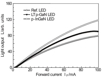 Figure 2. Light output power versus forward current for reference, LT p-GaN, and p-InGaN LEDs.
With current injection of 100mA, the p-InGaN LED outputs 45.2% more light than the reference device (Figure 2). The LT p-GaN LED only has 10.9% improved light output power compared with the reference at the same current.
The forward voltage of the p-InGaN LED at 20mA was 3.19V, a little higher than for the reference at 3.10V. By contrast, the LT p-GaN LED had a 3.39V forward voltage at the same current. High forward currents indicate resistive power losses and hence reduced efficiency.
The researchers blame the poorer contact between the ITO layer and p-contact where V-pits are present for the increased forward voltage. These losses are somewhat compensated for in the p-InGaN LED due to its lower-resistivity contact layer due to the higher hole density.
In terms of the angular distribution of the light output, the p-InGaN LED puts out more power at all angles compared with the other devices.
http://iopscience.iop.org/1674-1056/22/8/086803
The author Mike Cooke is a freelance technology journalist who has worked in the semiconductor and advanced technology sectors since 1997.
