


- News
8 April 2014
Improving electrically pumped external-cavity mode-locking
ETH Zürich and Philips Technologie GmbH have developed 981nm-wavelength passively mode-locked electrically pumped vertical-external-cavity surface-emitting lasers (EP-VECSELs) with “the shortest pulses (2.5ps), highest average output power (53.2mW), highest repetition rate (18.2GHz), and highest peak power (4.7W) to date” [C. A. Zaugg et al, Appl. Phys. Lett., vol104, p121115, 2014].
Mode-locking is a technique to produce extremely short laser pulses. The researchers believe that EP-VECSELs could drastically reduce the complexity, footprint and cost of such devices, with potential applications in optical communication, sampling and clocking. The researchers comment: “If optimized for compactness, the laser could be built in a volume as small as 1cm3 with little effort, and even smaller if industrial packaging would be applied.”
An EP-VCSEL consists of a gain chip and semiconductor saturable absorber mirror (SESAM) arranged in V- or Z-shape cavity configurations. The V-shape configuration includes a curved output coupler (OC). The Z-shape configuration has an added curved high-reflectivity (HR) mirror (Figure 1).
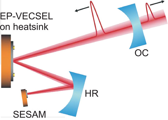
Figure 1: Z-cavity setup for EP-VECSEL.
The ETH/Philips team used both V- and Z-cavity setups. In the V-cavity configuration, the SESAM was placed about 3mm from the gain chip.
Philips Technologie fabricated the gain chip with an improved doping scheme for a better trade-off between electrical and optical losses, and implementing a smaller bottom contact than the top contact to strongly confine the current-injection profile in the center of the device. These factors optimized the fundamental mode (TEM00) of the cavity.
The gain chip was flipped so that the laser light was emitted through the growth substrate. The substrate was thinned to 100μm before flipping. The active light-emitting region consisted of three indium gallium arsenide (InGaAs) wells embedded in gallium arsenide (GaAs) barriers. The active region was sandwiched between distributed Bragg reflectors (DBRs). The bottom DBR (grown last) consisted of a 37-pair p-type structure. The top DBR was an 11-pair n-type structure.
The bottom contact was 60μm diameter. The chip was bonded to an aluminium nitride (AlN) heat spreader. The light-emitting oxide aperture was 100μm diameter with a ring electrode top contact. An anti-reflective coat was also applied.
The SESAM consisted of a 30-pair AlAs/GaAs DBR, single InGaAs quantum well in AlAs, and a thin GaAs cap. The InGaAs well was designed to be at an anti-node of the electromagnetic standing-wave field. Also, the semiconductor-air interface was at an electric field node (i.e. zero field). The SESAM was coated with silicon nitride and silicon dioxide using plasma-enhanced chemical vapor deposition (PE-CVD) to improve modulation depth and saturation fluence.
With a long V-cavity (13.3mm between gain chip and OC), the highest average output power of 53.2mW at 355mA injection current was achieved with mode-locking, resulting in a pulse repetition rate of 9.2GHz (Figure 2). The pulse duration was 2.9ps. The gain chip heat-sink was maintained at 3°C while the SESAM was at 32°C.
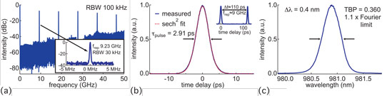
Figure 2: SESAM mode-locked EP-VECSEL with highest average output power of 53.2 mW. (a) Microwave spectrum of pulse train in wide span and zoomed in around fundamental pulse repetition frequency of 9.23GHz (inset). (b) Autocorrelation (blue) and sech2-fit (red dashed) revealing pulse duration of 2.9ps. Fundamental mode-locking with longer time delay (inset). (c) Optical spectrum. (TBP: time-bandwidth product.)
A short-cavity (5mm gain chip to OC) mode-lock of 18.2GHz repetition rate of 9.7ps pulses achieved an average output power of 10.1mW at 265mA. The gain chip heat-sink was at 3°C and the SESAM was at 25°C. The dimensions of the essential elements of this EP-VECSEL cavity setup were 3cmx3cmx2cm.
In a Z-cavity configuration, the pulses were as small as 2.47ps at 282mA injection current (10.6°C gain chip, 55°C SESAM). The average output power was 15.9mW. The repetition rate was 2.17GHz.
Table 1: Overview of EP-VECSEL results.
| Pavg (mW) | frep (GHz) | τpulse (ps) | Ppeak (W) |
| 53.2 | 9.2 | 2.91 | 1.74 |
| 10.1 | 18.2 | 9.48 | 0.05 |
| 15.9 | 2.2 | 2.47 | 2.62 |
| 35.0 | 2.2 | 3.03 | 4.73 |
Increasing the injection current to 288.7mA and reducing the gain chip temperature to 9.7°C increased the average output power to 35mW with 3ps pulses at 2.15GHz repetition. This configuration had the highest peak power of 4.7W (Table 1).
http://dx.doi.org/10.1063/1.4870048
The author Mike Cooke is a freelance technology journalist who has worked in the semiconductor and advanced technology sectors since 1997.


