


- News
28 April 2014
Strain and light emission in gallium arsenide nanowires
Researchers in Switzerland and Norway have used strain to alter the light-emitting properties of gallium arsenide (GaAs) nanowires [G. Signorello et al, Nature Communications, vol5, p3655, published online 10 Apr 2014]. The researchers from IBM Research-Zürich, Norwegian University of Science and Technology (NTNU) and CrayoNano AS found that different strain conditions cause a transition in the band structure from a direct bandgap to a pseudo-direct bandgap.
The GaAs nanowires were grown in the wurtzite (WZ) rather than the zincblende crystal structure that is usual with bulk GaAs. The researchers found bright photoluminescence under tension but decreasing brightness under compression. This is interpreted as signaling the transition between a direct to a pseudo-direct energy gap.
There are two conduction bands in WZ GaAs - one offering a direct gap with strong photon emission with transitions to the valence bands of heavy- and light-hole states and the other with simple photon emission to the light-hole band forbidden by symmetry considerations. The direct/pseudo-direct transition occurs when one of these gaps becomes smaller in energy than the other.
The researchers see the use of such strain effects as being potentially useful to increase carrier lifetime and quantum efficiency of photodetectors, as well as to decrease dark currents and generation-recombination noise. Further, they comment: “These results pave the way for a new generation of devices that can simultaneously serve as efficient light emitters and efficient photodetectors by leveraging the uniaxial strain degree of freedom.”
The researchers hope to combine these discoveries with nanowire growth methods on graphene developed by Crayonano to produce improved solar cells and light-emitting diodes (LEDs). NTNU and Crayonano also plan to grow gallium nitride (GaN) nanowires on grapheme, with a view to creating flexible, strong, lightweight white LEDs with better optical properties.
The c-axis wurtzite nanowires were produced in a molecular-beam epitaxy (MBE) reactor using a gold-catalyzed vapour-liquid-solid method. The nanowires consisted of a ~40nm GaAs core, and further shells of ~40nm Al0.3Ga0.7As and ~3nm GaAs. The core and AlGaAs shell are lattice-matched. The GaAs shell protects the structure from oxidation.
The nanowires were fabricated into free-standing structures clamped with titanium to a flexible substrate of stainless-steel covered in polymer (Figure 1). Bending the structure created tensile or compressive strain in the nanowire.
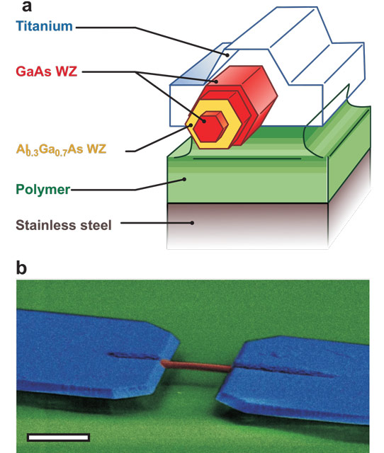
Figure 1: Wurtzite GaAs nanowire strain device. (a) Schematic cross-section of a nanowire strain device. Device dimensions are not to scale. (b) False-color scanning electron micrograph (SEM) of nanowire strain device. Scale bar is 1mm.
Under unstrained conditions, the researchers estimated an optical bandgap of 1.417eV±8meV (~875nm near-infrared wavelength) by using a model that combines data from Raman spectroscopy and photoluminescence (PL) with a k.p model of the strain-dependent effects on the energy bands (Figure 2). The temperature of the measurement was estimated to be in the range 300-480K due to laser-induced heating on the relatively thermally isolated nanowire structure.
Lead author Giorgio Signorello comments: “The laser power was chosen to be as low as possible for compatibility with the measurement of the PL spectra and, especially, of the Raman spectra (which impose the tightest requirements in terms of laser power). I want to emphasize that using the same laser power for PL and Raman is very important to plot correlated Raman/PL data in Figure 2.”
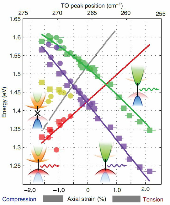
Figure 2: k.p model of uniaxial stress effects in wurtzite GaAs. Energy of optical transitions, extracted from fits of PL spectra are plotted as function of Raman transversal optical (TO) phonon peak position (top abscissa) and of inferred axial strain (bottom abscissa). Squares and circles represent the values obtained from two different nanowire devices. Continuous lines correspond to uniaxial strain dependence of photon energy expected from k.p model. Transitions between the bright conduction band and the heavy- and light-hole states are in purple and green, respectively. Transitions between dark conduction band and heavy-hole band are in red, whereas forbidden transitions between dark conduction band and light hole are represented by grey line. The researchers also found a dark transition (yellow data points) that follows a nonlinear energy shift that differs between the two nanowire devices “whose origin is not yet clear”.
The difference between the bright and dark conduction bands was estimated at 33meV±47meV. For comparison, zincblende (ZB) GaAs has a gap of 1.376eV±15meV for temperatures of 398±32K.
http://dx.doi.org/10.1038/ncomms4655
The author Mike Cooke is a freelance technology journalist who has worked in the semiconductor and advanced technology sectors since 1997.


