


- News
4 April 2014
Pushing high-power, high-frequency performance of GaN HEMTs on silicon
Singapore’s Nanyang Technological University has developed conventional aluminium gallium nitride (AlGaN) high-electron-mobility transistors (HEMTs) with record-breaking figures-of-merit (FOMs) for frequency and breakdown performance [Kumud Ranjan et al, Appl. Phys. Express, vol7, p044102, 2014].
The Johnson FOM is defined as the product of the unity current gain cut-off frequency and the off-state breakdown gate-drain voltage (fTxBVgd). The J-FOM is designed to reflect the needs of high-power microwave devices. The Nanyang device achieved 8.32THz-V, which is claimed as a record for conventional T-gate AlGaN/GaN HEMTs on silicon substrates (Figure 1). Using much more expensive silicon carbide (SiC) substrates, researchers in Japan produced HEMTs with 12.9THz-V J-FOMs.
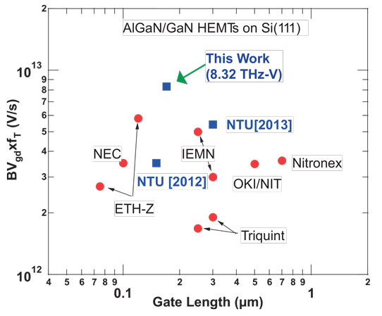
Figure 1: Benchmarking with state-of-the-art J-FOMs (BVgdxfT) versus Lg for AlGaN/GaN HEMTs on Si substrates.
The conventional AlGaN/GaN HEMT structures (Figure 2) were grown on 100mm high-resistivity (111) silicon substrates using metal-organic chemical vapor deposition (MOCVD). The resulting two-dimensional electron gas (2DEG) channel had a carrier density of 0.87x10¹³/cm2 with mobility of 1940cm2/V-s.
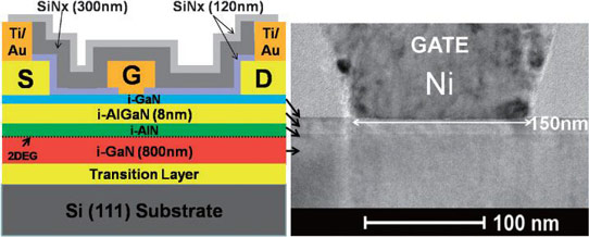
Figure 2: Schematic cross-section and high-resolution cross-sectional transmission electron micrograph (TEM) (gate region) of Nanyang AlGaN/GaN HEMTs on Si substrates.
In more detail, the layer structure consisted of 100nm AlN nucleation, 1400nm transition, 800nm GaN buffer/channel, 1nm AlN spacer, 8nm Al0.26Ga0.74N barrier, and 2nm GaN cap. The AlN spacer improved the mobility of the 2DEG to allow higher frequencies and transconductance. The thin AlGaN barrier reduced short-channel-effect performance degradation.
The HEMT fabrication used plasma etch for mesa isolation, annealed titanium/aluminium/nickel/gold for ohmic source-drain contacts, ammonium sulfide ((NH4)2Sx) treatment, T-gate formation, titanium/gold transmission lines, and silicon nitride passivation. The T-gate footprint measured 0.15μm. The T-head was 0.5μm. Further device dimensions were 0.8μm source-gate, 2x75μm gate width, and 3μm gate-drain.
The maximum DC current of the device was 800mA/mm. The peak extrinsic transconductance was 346mS/mm. The threshold voltage was −1.7V. The drain-induced barrier lowering (DIBL) was “negligibly small” at 1.5-3.0mV/V. This compares with DIBL values an order of magnitude greater achieved with ~0.15μm gates and InGaN or AlGaN back barriers. The researchers comment on their device: “The observed low DIBL is due to the large gate-to-channel aspect ratio (Lg/dgc ~ 15).”
Small-signal high-frequency measurements gave estimates for the cut-off frequency (fT) of 63.1GHz and the maximum oscillation/unity power gain (fmax) of 124GHz for 6V drain and −0.8V gate biasing. The three-terminal off-state 1mA/mm breakdown (BVgd) occurred at 132V.
Current collapse under gate- and drain-lag pulsed operation was 6% and 8%, respectively. The researchers comment: “These values are closely matched with or even better than those in other reports on AlGaN/GaN HEMTs on Si substrates. The suppression of current collapse is mainly due to the ammonium sulfide treatment plus SiN passivation.”
GaN HEMTs on silicon GaN AlGaN HEMTs
http://iopscience.iop.org/1882-0786/7/4/044102/article
The author Mike Cooke is a freelance technology journalist who has worked in the semiconductor and advanced technology sectors since 1997.


