


- News
21 August 2014
Fukuda Crystal Lab grows 2-inch scandium aluminium magnesium oxide crystal rivalling sapphire
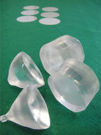
Fukuda Crystal Laboratory Co Ltd has grown ScAlMgO4 scandium aluminium magnesium oxide (SCAM) crystal with a diameter of 50mm (2 inches) that could be used as a substrate for gallium nitride (GaN)-based light-emitting devices such as blue LEDs and blue-violet laser diodes.
The lab says that, compared with sapphire (often used as a blue LED substrate), SCAM is suited to reducing crystal defects in GaN-based semiconductors. SCAM is hence expected to improve the brightness of light-emitting devices.
 A research group led by professor Takashi Matsuoka of Tohoku University’s Institute for Materials Research formed a GaN-based LED structure using the prototype crystal, and confirmed that the effect was to improve the brightness.
The lattice mismatch between SCAM and GaN is as small as 1.8%, and SCAM causes few dislocation crystal defects. Although it is difficult to make the SCAM crystal, Fukuda Crystal Laboratory has grown the 2-inch SCAM crystal by the Czochralski (CZ) method, improving the crystal quality by tailoring the furnace structure and changing the crystal growth conditions.
When the prototyped SCAM crystal was cleaved and its C surface examined by x-ray diffraction, its full width at half maximum (FWHM) was 12.9 seconds, which is equivalent to the quality of a perfect silicon (Si) crystal, it is claimed.
Also, Fukuda Crystal Laboratory fabricated the wafer just by cleaving an ingot of SCAM crystal without cutting or polishing it, making it possible to lower the cost of wafers. When a thin film of GaN was grown on the cleaved surface of the SCAM crystal by metal-organic chemical vapor deposition (MOCVD) at a temperature of 1040°C, a low-dislocation crystal with a mirror surface was formed.
Fukuda Crystal Laboratory plans to increase the diameter of the SCAM crystal and commercialize it. Specifically, it intends to launch a 2-inch SCAM substrate by spring 2015.


