


- News
25 August 2014
Scaling III-V integration to 300mm-diameter silicon and beyond
Researchers based in Japan and USA have reported further details of a direct wafer bonding (DWB) technique that could open the way to integration of indium gallium arsenide (InGaAs) high-mobility electronics and optoelectronics on the largest-diameter wafers available [SangHyeon Kim et al, Appl. Phys. Lett., vol105, p043504, 2014]. The team from University of Tokyo, JST-CREST funding program, and IntelliEPI has previously presented some details of the process at the 2014 VLSI Symposium [Cooke, Semiconductor Today, p78, June/July 2014].
The researchers believe that their DWB process offers a combination of wafer scalability to more than 300mm, tight integration with silicon devices, and channel layer quality that is not matched by the competing integration methods (Table 1).
Table 1: Comparison among integration schemes of III-V MOSFETs on Si wafer.
| Integration method | Wafer-level epitaxy | Epitaxial transfer | Aspect ratio trapping | Wafer bonding with Si donor |
| Structure | III-V channel/thick buffer/Si | III-V-OI | III-V/Si with trench | III-V-OI |
| Short-channel-effect control | Finfet | Ultra-thin body | Finfet | Ultra-thin body |
| Water scalability to 300mm | + | − | + | + |
| Tight integration with Si device | − | + | − | + |
| Channel layer quality | + | + | − | + |
Generally, DWB and other epitaxial transfer techniques use a donor wafer where the InGaAs or other III-V semiconductor channel layer is grown on a III-V material such as indium phosphide (InP). However, this limits the ability to integrate with large-diameter silicon wafers. While III-V substrates are often limited to 2-inches and less, the maximum silicon wafer diameter is 300mm commercially, with 450mm in development.
The Japan/US team has overcome the limitation by creating a donor wafer on 4-inch silicon wafers using molecular beam epitaxy (MBE). The technique is therefore not constrained by the limitations of III-V crystal growing technology.
The buffer between substrate and InGaAs channel layer (Figure 1) consisted of gallium arsenide (GaAs) followed by graded indium aluminium arsenide (InAlAs). Various thicknesses up to 50nm for the In0.53Ga0.47As channel layer were produced. Room-temperature Hall measurements gave 6550cm2/V-s mobility and 1.5x10¹⁷/cm3 carrier concentration.
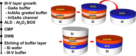
Figure 1: Fabrication of InGaAs-OI wafer by DWB technique using Si donor wafer.
The wafer bonding was prepared by applying aluminium oxide (Al2O3) by atomic layer deposition (ALD) to both the donor and final wafers. Chemical mechanical polishing (CMP) was used to smooth the wafers. The bonding was performed after further ALD of hafnium dioxide (HfO2).
The InGaAs channel layer on oxide insulator was finally revealed by etching away the silicon donor wafer and the GaAs and InAlAs buffer layers with tetramethylammonium hydroxide (TMAH), citric acid, and hydrochloric acid solutions, respectively.
The researchers believe that alternative methods of substrate removal could be implemented, such as hydrogen-induced thermal wafer splitting. The researchers add that such wafer splitting processes would be expected to significantly reduce process costs through recycling of the donor wafer.
Infrared photography showed a good, uniform bond with no voids present. Raman and photoluminescence spectral analyses showed very similar performance of layers produced with silicon or indium phosphide donor substrates.
The root-mean-square surface roughness of the InGaAs layer was 1.4nm, according to atomic force microscopy (AFM). Transmission electron microscopy (TEM) gave images with no dislocations and fast Fourier transform analysis of the image suggested good crystal quality.
Metal oxide semiconductor field-effect transistors (MOSFETs) were fabricated with Al2O3 oxide and tantalum metal gate stack on 9nm InGaAs-on-insulator (InGaAs-OI) body. The source/drain contacts were nickel/InGaAs. With a 1μm gate length, the subthreshold swing was 100mV/decade and the on/off current ratio more than 106. The peak transconductance was around 100μS/μm.
The effective mobility of MOSFETs on varying body thickness increases to 1700cm2/V-s at 50nm (Figure 2). At 9nm body thickness, the effective mobility is still an improvement on Si MOSFETs. The 50nm mobility is 3x that of Si-based devices. The mobility for silicon donor wafer devices was comparable to that of MOSFETs produced using InP donor wafers. The researchers comment: “These results strongly suggest that high-quality InGaAs-OI can also be fabricated from Si donor wafers.”
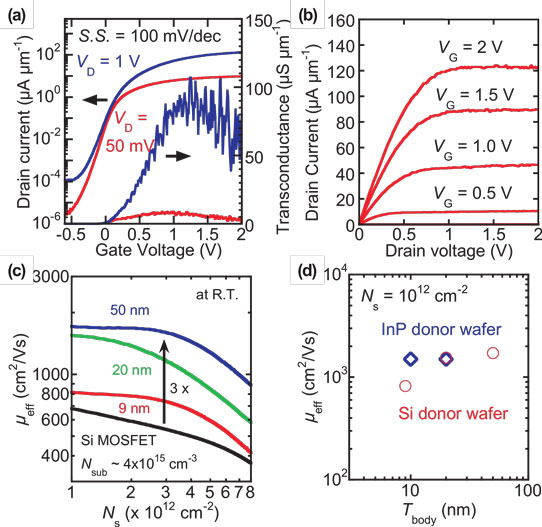
Figure 2: (a) Measured transfer and (b) output characteristics of InGaAs-OI MOSFETs. (c) Effective mobility characteristics of InGaAs-OI MOSFETs with 9nm, 20nm, and 50nm body thickness, and of reference Si MOSFET. (d) The effective mobilities of InGaAs-OI MOSFETs from InP and Si donor wafer versus body thickness.
The drain current versus gate voltage performance at 50mV drain was very uniform across 35 1μm gate MOSFETs. The leakage current was also as low, if not lower, as for a similar sample of InP-donor-wafer MOSFETs. Both these indicators suggested that good, uniform-quality channel layers had been achieved.
Direct wafer bonding InGaAs IntelliEPI MOSFETs InP MBE
http://dx.doi.org/10.1063/1.4891493
The author Mike Cooke is a freelance technology journalist who has worked in the semiconductor and advanced technology sectors since 1997.


