


- News
1 August 2014
Silicon carbide bipolar opamp performance at 500°C
Sweden’s Royal Institute of Technology (KTH) has created a monolithic operational amplifier circuit using 4H polytype silicon carbide (SiC) bipolar junction transistors (BJTs) [Raheleh Hedayati et al, IEEE Electron Device Letters, vol35, p693, 2014]. The researchers see applications for such devices that can potentially operate at up to 600°C as being in “Venus exploration, oil and gas drilling, aviation, and automotive”.
Although SiC junction field-effect transistors (JFETs) have been reported as working at up to 576°C (Table 1), BJTs have higher speed, better linearity, and higher drive current. Metal-oxide-semiconductor (MOS) transistors are limited by the stability of the oxide layer to temperatures of 400°C and less.
Table 1: Comparison of high-temperature opamps in silicon carbide.
| Technology | Temperature | Open-loop gain | Gain bandwidth |
| 4H-SiC MOSFET | 300°C | 57dB | - |
| 6H-SiC MOSFET | 300°C | 53dB | 269kHz |
| 6H-SiC JFET | 576°C | 69dB | 1400kHz |
| 4H-SiC bipolar (KTH) | 500°C | 64dB | 4360kHz |
The NPN bipolar transistors were fabricated on a 4-inch 4H-SiC substrate with six epitaxial layers of varying doping concentrations (Figure 1). The mesas for the emitter, collector and base regions were achieved using plasma etch. The ~0.01mm2 devices achieved maximum current gains (β = collector/base currents) of 38 at 25°C and 15 at 500°C.
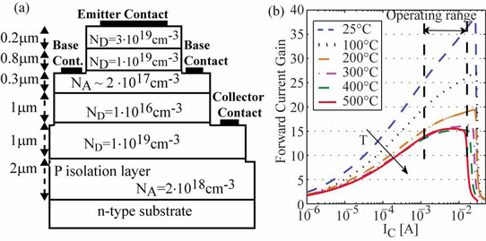
Figure 1: (a) Cross-sectional schematic and microphotograph of SiC NPN transistor. (b) Measured β versus collector current of NPN transistor from 25°C to 500°C.
The researchers used 17 transistors to create an opamp IC (Figure 2) with two gain stages, buffers, level shifter, and an output stage. The power supply was a dual ±7.5V system. The operating points for the transistors in the circuit varied between 0.4mA (22 gain at room temperature) at the input and 14mA for the output (36 gain).
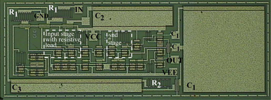
Figure 2: Microphotograph of opamp with integrated feedback resistor (total area ∼3.75mm2).
The researchers had integrated a 30pF capacitor to provide ‘Miller compensation’ for the closed-loop circuit, giving an inverting negative feedback amplifier configuration, but found that a 330pF capacitor off-chip was also needed for stability. The trade-off was smaller bandwidth. External components such as the off-chip capacitor and load resistor/capacitor were kept at room temperature.
Although the closed-loop gain and gain bandwidth degrade between 25°C and 500°C, the 3dB-bandwidth (‘half-power point’) increases (Table 2). The researchers attribute the wider 3dB-bandwidth to the reduction in bias resistance leading to increased cut-off frequencies of the transistors. Also, the slew rate increases at high temperature.
Table 2: Some measured performance criteria of KTH inverting opamp.
| 25°C | 500°C | |
| DC closed-loop gain with 500Ω load | 39.86dB | 39.46dB |
| Gain bandwidth | 5.92MHz | 4.36MHz |
| 3dB-bandwidth | 270kHz | 410kHz |
| Estimated open-loop gain | 76.3dB | 64dB |
| Positive/negative slew rates | 1.46/1.25V/μsec | 1.46/2.16V/μsec |
| Total harmonic distortion | -52dB/0.25% | -50dB/0.3% |
While the researchers estimate that the open-loop gain of the device decreases significantly between 25°C and 500°C, the closed-loop gain is remarkably stable over the wide temperature range.
http://dx.doi.org/10.1109/LED.2014.2322335
The author Mike Cooke is a freelance technology journalist who has worked in the semiconductor and advanced technology sectors since 1997.


