


- News
8 August 2014
Passivating nitride transistors without vacuum processing
Researchers in Taiwan have applied a non-vacuum process to deposit aluminium oxide (Al2O3) passivation for nitride semiconductor high-electron-mobility transistors (HEMTs) [Bo-Yi Chou et al, IEEE Electron Device Letters, published online 11 July 2014].
Normally, Al2O3 is deposited on aluminium gallium nitride (AlGaN) or gallium nitride using vacuum processes such as atomic layer deposition (ALD), metal-organic chemical vapor deposition (MOCVD), or plasma-enhanced chemical vapor deposition (PECVD). The necessity to pump down to vacuum conditions increases process time.
To avoid vacuum processing, researchers at National Cheng Kung University, Feng Chia University, and Industrial Technology Research Institute (ITRI) used ultrasonic spray pyrolysis deposition (USPD) – a technique that has been used for silicon-based solar cell and humidity sensor fabrication, but not previously for GaN HEMTs. The team comments: “The USPD technique possesses advantages of cost-effectiveness, reduced processing time, and non-vacuum environment.”
The researchers used epitaxial material grown on silicon carbide (SiC) using low-pressure MOCVD. The barrier layer was 25nm Al0.25Ga0.75N and the buffer/channel was 2μm GaN.
The transistor fabrication involved cleaning, mesa isolation, source/drain contact (Ti/Al/Ni/Au) deposition and annealing, and gate formation and passivation. Three types of device were produced: unpassivated, and passivated with Al2O3 or Si3N4. The unpassivated device was annealed at 350°C for six minutes, mimicking the growth condition for the Al2O3 passivation. The 100nm Si3N4 was applied using 300°C PECVD.
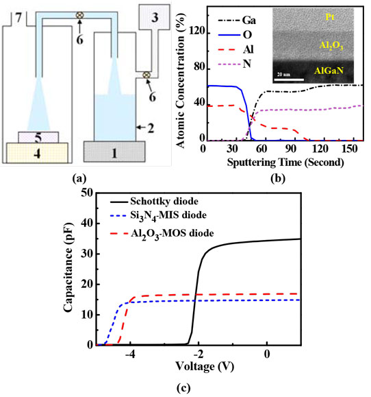
Figure 1: (a) Schematic of USPD system: (1) ultrasonic atomizer, (2) precursor solution, (3) carrier gas supply system, (4) heater, (5) sample holder, (6) controller, and (7) exhaust. (b) Atomic concentration of the studied sample by using electron spectroscopy for chemical analysis (ESCA) and, inset, transmission electron microscope (TEM) photo of Al2O3/AlGaN. (c) C-V characteristics of diodes.
The USPD process (Figure 1) for Al2O3 deposition involved aluminium acetylacetonate dissolved in water/ethanol. The precursor was atomized using ultrasound and transported to the 350°C heated substrate in nitrogen carrier gas. At the substrate the aluminium acetylacetonate decomposes to give Al2O3. The resulting layer was 20nm, deposited at the rate 3.5nm/minute. On a 4-inch substrate the thickness uniformity was ±0.7nm.
Capacitance-voltage (C-V) measurements on metal-insulator-semiconductor diodes gave dielectric constants of 7.13 and 9.32, respectively, for Si3N4 and Al2O3 layers. The corresponding leakage currents under fields of 1MV/cm were 4.8x10⁻⁶A/cm2 for Si3N4 and 2.2x10⁻⁸A/cm2 for Al2O3. The unpassivated Schottky diode structure had a current leakage under reverse bias of 1.5x10⁻⁶A/cm2. The areas of the test diodes were 8000μm2. The interface trap densities (Dit) were estimated at 5.5x10¹¹/cm2-eV for Al2O3, compared with 9.7x10¹¹/cm2-eV for Si3N4.
Hall measurements (Table 1) showed reduced sheet resistance (RSH) with Al2O3 passivation. The improvement is attributed to increased carrier sheet density (ns) that more than compensates for a slightly reduced electron mobility (μn) due to carrier-carrier scattering. The researchers comment: “The obtained higher ns-μn product and lower RSH are advantageous to enhance the current drive ability for the present design.”
Table 1: Hall measurement parameters and DC and AC characteristics.
| Sample | A | B | C |
| Passivation | None | Si3N4 | Al2O3 |
| Hall measurements | |||
| Carrier density | 1.07x10¹³/cm2 | 1.15x10¹³/cm2 | 1.25x10¹³/cm2 |
| Electron mobility | 1270cm2/V-s | 1250cm2/V-s | 1235cm2/V-s |
| Sheet resistance | 460Ω/square | 434Ω/square | 404Ω/square |
| DC measurements | |||
| Maximum drain current | 552.7mA/mm | 629.2mA/mm | 686.6mA/mm |
| Drain current at 0V gate | 337.6mA/mm | 384.2mA/mm | 421.7mA/mm |
| On resistance | 10.94Ω-mm | 9.5Ω-mm | 8.65Ω-mm |
| Source resistance | 2.4Ω-mm | 2.2Ω-mm | 2Ω-mm |
| Drain resistance | 7.3Ω-mm | 6.3Ω-mm | 5.9Ω-mm |
| Peak transconductance | 114.1mS/mm | 131.3mS/mm | 152.4mS/mm |
| Off breakdown for 1mA/mm source-drain current and -6V gate | 75V | 70V | 109V |
| Gate-drain breakdown for 1mA/mm gate-drain current | -103.8V | -94.5V | -152.4V |
| 2.4GHz measurements at 15V drain bias and -2V gate potential | |||
| Maximum output power | 18.5dBm | 19.3dBm | 20.5dBm |
| Power added efficiency | 25.1% | 29.4% | 33.6% |
The HEMTs were formed by etching the Al2O3 with phosphoric etch. The gate length was 1μm and the width was 100μm. The gate spacing from the source/drain contacts was 2μm.
A variety of DC, AC and pulsed measurements were made. The researchers comment: “In comparison with unpassivated and Si3N4-passivated devices, reduced Dit, decreased leakage current, enhanced drain current density, relieved RF drain current collapse, and improved power performance are achieved at the same time for the present Al2O3-passivated HEMT design.”
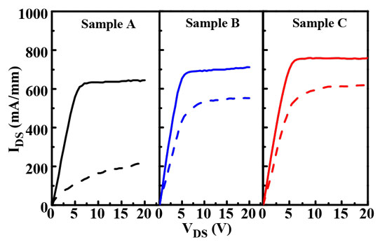
Figure 2: Pulsed drain current-bias (IDS-VDS) characteristics of samples A-C with quiescent-bias points of (VDS0, VGS0) = (0V, 0V) (solid lines) and (10V, -4V) (dash lines).
According to the researchers, the reduced current collapse (Figure 2) “indicates that the surface traps in the gate-to-drain/source regions have been effectively suppressed by using the USPD-grown Al2O3 passivation layer.”
GaN HEMTs GaN AlGaN SiC ALD MOCVD PECVD
http://ieeexplore.ieee.org/xpl/articleDetails.jsp?arnumber=6853327
The author Mike Cooke is a freelance technology journalist who has worked in the semiconductor and advanced technology sectors since 1997.


