


- News
27 August 2014
Graded electron blocking improves III-nitride VCSEL performance
Researchers in Taiwan have used graded electron-blocking layers (GEBLs) to improve the performance of III-nitride compound semiconductor vertical-cavity surface-emitting laser (VCSEL) diodes [B C Lin et al, Laser Phys. Lett., vol11, p085002, 2014]. The team was variously based at National Chiao Tung University, National Changhua University of Education, Advanced Optoelectronic Technology Inc, and Research center for Applied Science.
Most III-nitride light-emitting devices employ electron-blocking layers of aluminium gallium nitride (AlGaN) to confine electrons to the active multiple quantum well (MQW) regions where it is desired they should recombine with holes in the valence band, producing photons. However, electron-blocking layers (EBLs) often have the undesired side-effect of inhibiting hole injection.
The epitaxial III-nitride structures (Figure 1) used by the Taiwan team were grown on c-plane sapphire using metal-organic chemical vapor deposition (MOCVD). The n-side distributed Bragg reflector (DBR) consisted of 25 pairs of AlN/GaN layers.
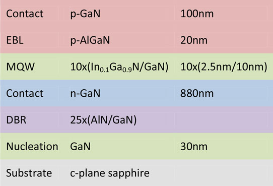
Figure 1: Epitaxial structure.
The EBL consisted of either ungraded p-Al0.25Ga0.75N or p-AlGaN graded from 0% to 25% Al composition. The grading of the AlGaN composition was achieved by varying the Al/Ga precursor ratio. The deposition temperature was 870°C in both ungraded and graded AlGaN deposition. The alternative grading technique of growth temperature variation was not adopted, since it could damage the previously grown MQW structure.
Transmission electron microscope (TEM) images of the interface between the last GaN barrier of the MQW and the ungraded EBL showed several abnormal dark regions. Such dark regions tend to be associated with degradation of crystal material quality. By contrast, dark regions were not apparent in the GEBL.
Simulations suggested that the effect of the GEBL was to provide a flatter profile in the valence band, while increasing the effective barrier in the conduction band, in comparison with the ungraded EBL. The flatter valence profile reduces the barrier for hole injection. The higher conduction-band barrier makes the EBL more effective at confining the electrons to the MQW active region. The positive effects of the GEBL are thought to be due to the reduced polarization charge density at the interface with the last GaN barrier of the MQW, where the Al-composition of the GEBL starts at 0%.
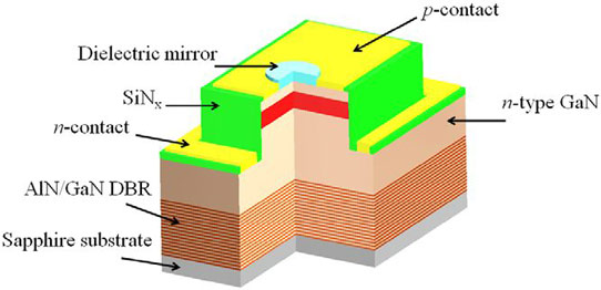
Figure 2: Schematic of InGaN-based VCSEL structure.
Fabrication of the VCSEL (Figure 2) involved plasma-enhanced CVD of silicon nitride (SiNx) for current confinement, opening of a 10μm-diameter current aperture, deposition and annealing of 40nm indium tin oxide (ITO) as a transparent current-spreading layer in the aperture, deposition of n- and p-contact electrodes (nickel/gold and titanium/aluminium/nickel/gold, respectively), and completion with the deposition of 10 pairs of tantalum pentoxide and silicon dioxide dielectrics to give the p-side DBR. Both DBRs give about 99% reflectivity at the peak emission wavelength of 410nm.
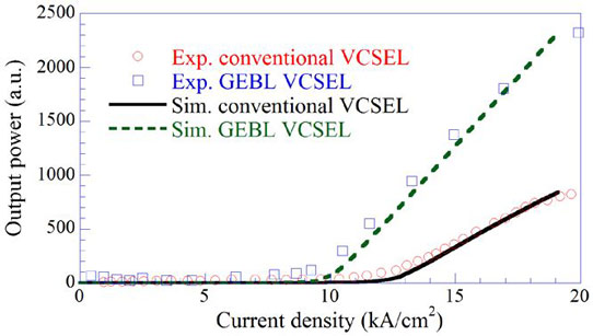
Figure 3: Laser performance of VCSELs with conventional rectangular EBL and GEBL obtained by experiment and numerical simulation.
The researchers compared their simulations with measurements made at 300K in continuous wave (CW) operation. The GEBL device shows a reduced threshold current density of 9.2kA/cm2, compared with 12.6kA/cm2 for the ungraded EBL VCSEL. The GEBL device also shows higher slope efficiency. At 20kA/cm2, the laser output power is a factor of 3.8 times that of the ungraded EBL VCSEL.
VCSEL AlGaN InGaN VCSEL GEBLs MOCVD
http://dx.doi.org/10.1088/1612-2011/11/8/085002
The author Mike Cooke is a freelance technology journalist who has worked in the semiconductor and advanced technology sectors since 1997.


