


- News
15 August 2014
Grading InGaN wells to increase LED light output power and efficiency
Singapore’s Nanyang Technological University and Turkey’s Bilkent University have developed a graded multiple quantum well (MQW) structure with the aim of increasing light output power and reducing efficiency droop in 450nm indium gallium nitride (InGaN) light emitting diodes (LEDs) [Zi-Hui Zhang et al, Appl. Phys. Lett., vol105, p033506, 2014].
The use of graded InGaN composition allowed wider wells to be created in the hope of reducing carrier densities so that, in turn, Auger recombination is reduced. Auger recombination is a non-radiative mechanism where the energy from electron-hole transitions is transferred to another carrier (electron or hole) rather than being emitted as a photon. Such a mechanism becomes more significant as carrier densities increase.
Commercial InGaN LEDs use MQWs with abrupt wells of InGaN with GaN or low-indium-content InGaN barriers. The thickness of abrupt InGaN wells is limited to around 3nm due to crystal quality considerations. The grading technique allowed the Nanyang/Bilkent team to increase the thickness to 5nm.
The aim of the design was to increase the light output power while reducing efficiency droop effects. Often, changes aimed at reducing efficiency droop do so at the cost of peak efficiency.
The epitaxial structures (Figure 1) were grown on c-plane sapphire through metal-organic chemical vapor deposition (MOCVD). Two device structures with different MQW designs were produced – one without composition grading and the other with.
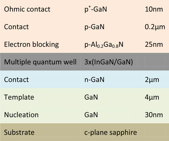
Figure 1: Schematic epitaxial structure.
The standard non-graded three-period MQW (‘sample A’) consisted of 3nm In0.15Ga0.85N wells in 12nm GaN barriers. The graded structure (‘sample B’) used composition grading between 8% and 15% indium to give the wider 5nm well. The barrier thickness was kept at 12nm. The target peak emission wavelength of both structures was 450nm.
The researchers also believe that another effect of grading would be to reduce the polarization-induced interface charge density from around 0.54x10¹⁷/m2 to 0.3x10¹⁷/m2 (Figure 2). At the same time, the grading also introduces a bulk charge density in the well of 5.15x1024/m3. Therefore the electric field in the well is reduced and, along with it, the quantum-confined Stark effect that creates a tendency for the electrons and holes to be pulled apart, reducing light emission.
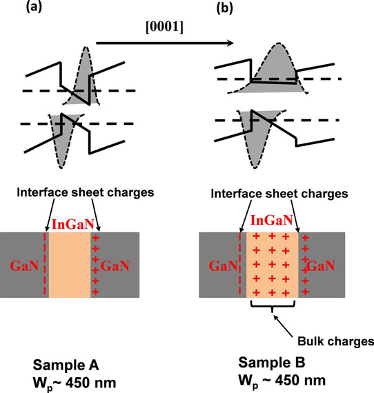
Figure 2: Schematic energy diagrams for quantum well region of (a) conventional LED sample A and (b) proposed LED sample B with wide quantum well and InN composition linearly decreasing along the [0001] growth orientation.
These changes are therefore expected to increase the overlap of the electron-hole wavefunctions and hence to increase recombination into photons. Also, by allowing wider wells, the grading reduces carrier concentration for a given current injection, decreasing the non-radiative Auger recombination route.
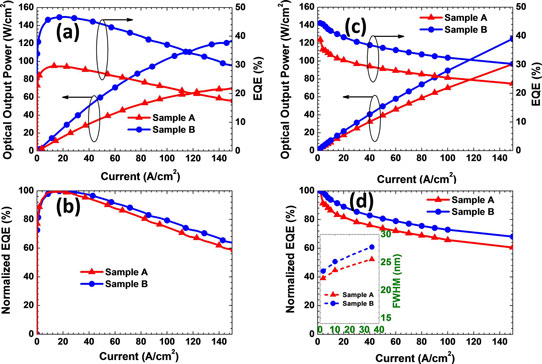
Figure 3: (a) Numerically computed optical output power and EQE, (b) calculated normalized EQE, (c) experimentally measured optical output power and EQE, and (d) measured normalized EQE, and (inset) full-width at half maximum (FWHM) versus current density.
Electroluminescence measurements in an integration sphere with 1mm-diameter indium metal contacts to the n- and p-type regions of the device showed increased output power and efficiency for sample B, in line with the researchers’ simulations (Figure 3). At 150A/cm2 injection current, the LED based on sample B showed a 29.39% increase in optical output power, compared with a sample A device. At the same injection, the devices’ droop in external quantum efficiency (EQE) from the peak value was 39.23% for sample A and 31.83% for sample B.
LEDs Auger recombination InGaN wells InGaN MOCVD
http://dx.doi.org/10.1063/1.4891334
The author Mike Cooke is a freelance technology journalist who has worked in the semiconductor and advanced technology sectors since 1997.


