


- News
10 December 2014
Resistance memory with all-nitride structure
Chinese Academy of Science researchers have developed a memory resistor (memristor) based on III-nitride semiconductors with a metal-insulator-semiconductor (MIS) structure [Yiren Chen et al, Appl. Phys. Lett., vol105, p193502, 2014].
The team from State Key Laboratory of Luminescence and Applications, Changchun, believes that the structure could result in monolithic integrated one-transistor-one-resistor (1T1R) memory in conjunction with III-nitride high-electron-mobility transistors (HEMTs).
Similar devices are being developed in mainstream silicon technologies as an alternative to the capacitance-based structures used commercially.
The nitride memristor had two resistance levels that could be set or reset to provide bipolar memory states. The device (Figure 1) was based on an n-type aluminium nitride (AlN) on gallium nitride (GaN) structure grown on c-plane sapphire through metal-organic chemical vapor deposition (MOCVD).
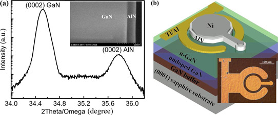
Figure 1: (a) (0002) plane 2& theta;-& omega; scan of AlN/n-GaN structure x-ray analysis. Inset: cross-sectional SEM image. (b) Schematic configuration of AlN/n-GaN MIS device. Inset: metallographic micrograph of MIS cell.
The sapphire was subjected to thermal desorption of hydrogen before the MOCVD processing. The GaN consisted of a 36nm low-temperature 550°C nucleation layer, 1μm of undoped buffer material, and 200nm of silicon-doped n-GaN. The non-nucleation layers were grown at 1050°C. The final 80nm AlN insulator layer was grown at 1100°C.
The memory device was fabricated by creating an AlN mesa through inductively coupled etch, depositing and annealing a titanium/aluminium ohmic electrode on the n-GaN surface and a Schottky nickel contact on the AlN mesa.
Decreasing the voltage across the device to -8V caused the structure to switch from a high resistance state (HRS) to a low resistance state (LRS) at -3V (Figure 2). The researchers designated this as the ‘SET’ process. ‘RESET’ occurred through sweeping up through a negative differential resistance region between +1.7V and +2.2V.
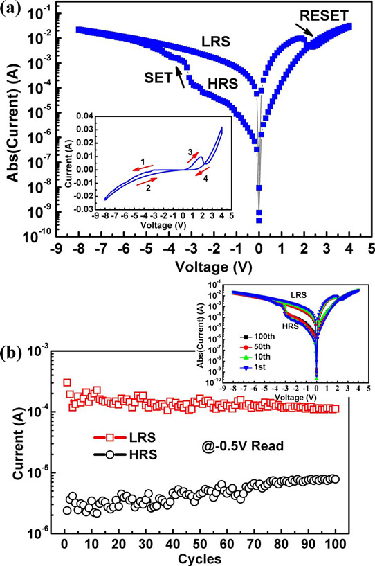
Figure 2: (a) Typical current-voltage (I-V) curve of pristine AlN/n-GaN MIS device shown in semi-logarithmic scale. Direction pointed by red arrows numbered 1 to 4 in inset is sequence of sweeping voltage. (b) Endurance performance of AlN/n-GaN MIS device. Inset: representative I-V curves of 100 sweeping cycles.
Repeating the SET/RESET processes for 100 cycles with -0.5V as the reading voltage, the researchers found a “slight” degradation in the separation between the LRS and HRS. This is attributed to increased leakage through dislocations in the III-nitride materials. The researchers say that the device needs improvement in this respect.
The researchers, on the basis of space-charge-limited current theory, believe the memristor effect is related to traps in the AlN layer. The AlN growth temperature of 1100°C is relatively low, leading to a large number of traps.
Analysis of temperature-dependent measurements suggested that the traps were mainly nitrogen vacancy energy levels. The researchers also think that the charge polarization of the chemical bond in AlN creates an electric field that tilts the potential wells of the traps, facilitating transport of injected carriers.
Negative voltages fill up the traps, allowing a hopping current. A positive voltage bends the GaN conduction band downward toward the AlN interface, creating a well where electrons accumulate, inhibiting current flow by space-charge effects. Also, the field direction enhances the tilting arising from the spontaneous polarization. The trap levels empty, cutting off the hopping current.
Memory resistor HEMTs GaN MOCVD
http://dx.doi.org/10.1063/1.4901747
The author Mike Cooke is a freelance technology journalist who has worked in the semiconductor and advanced technology sectors since 1997.


